


🔥 Explore this awesome post from Hacker News 📖
📂 **Category**:
💡 **What You’ll Learn**:
Spacelab was a reusable laboratory that could be carried in the Space Shuttle’s cargo bay, providing lab space for astronauts
and experiments.1
Because Spacelab was a European project, it used a French-built minicomputer, the Mitra 125 MS,2
rather than the Shuttle’s main computers, IBM-built AP-101 systems.
For storage, the Spacelab computer contained 128 kilobytes of RAM.
Rather than silicon memory, the computer used magnetic core memory, with each bit stored in a tiny ferrite ring.
In this article, I take a close look at this computer’s core memory system.
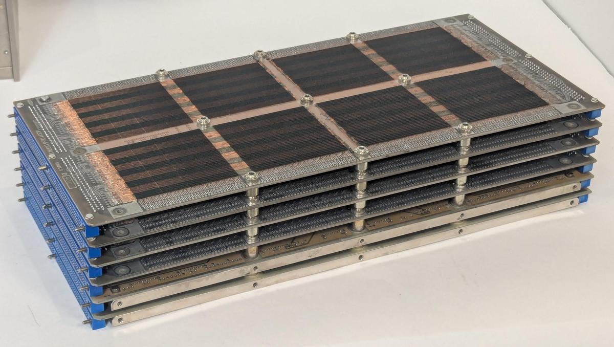
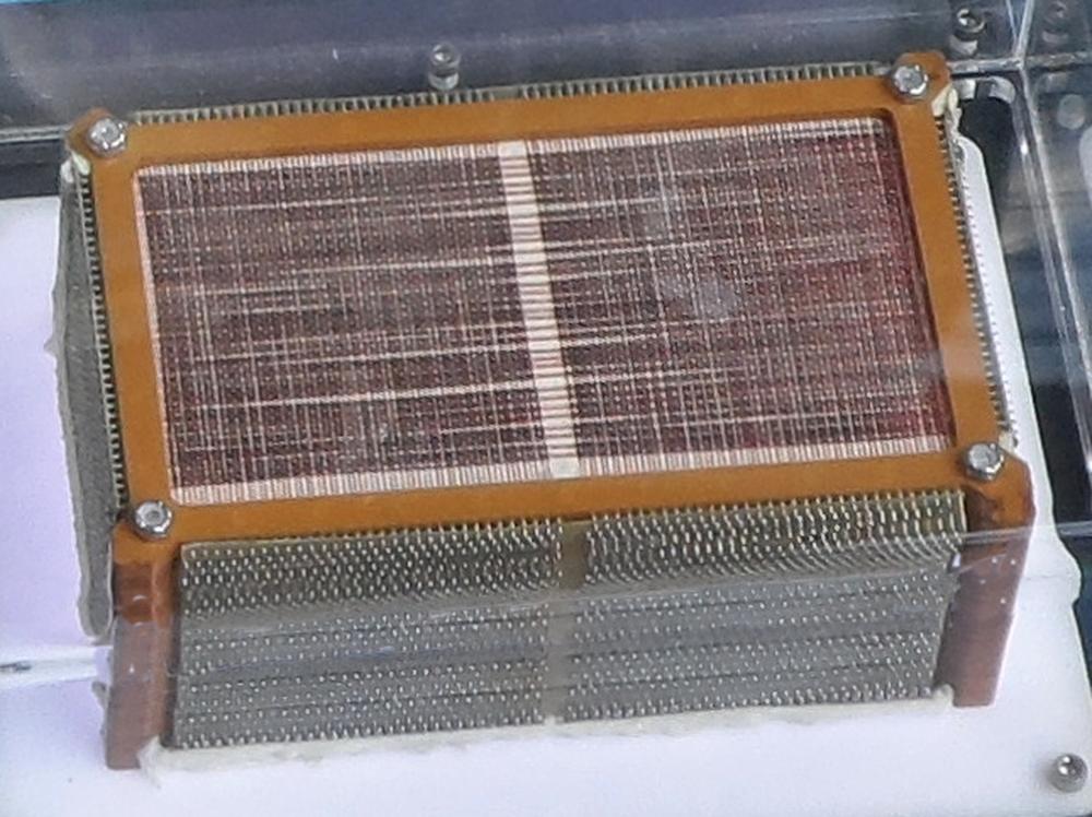
The core stack from the Spacelab computer. I removed the top board to show the core planes.
The illustration below shows how Spacelab fit inside the Shuttle’s cargo bay.
The pressurized laboratory is the cylindrical module in the front of the cargo bay, connected to the Shuttle by a tunnel.
Experiments were mounted on pallets behind the laboratory.
The laboratory held three identical Mitra computers.3 One computer
managed Spacelab itself, while the second computer managed the experiments. The third computer provided a backup in case of failures.
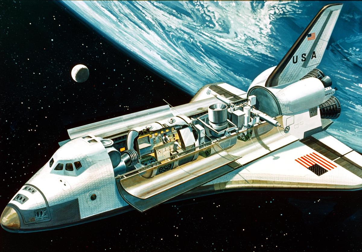
Spacelab was a pressurized cylinder in the Shuttle’s cargo bay, connected to the Shuttle by a tunnel. It provided a laboratory for researchers to perform experiments. This illustration of Spacelab is from NASA, C-1976-4380.
The photo below shows the core memory stack, removed from the computer.
The core memory stack takes up roughly a third of the computer. The entire side panel of the computer detaches, and the core
memory unit slides out.
Since the computer is cooled by conduction, firmly attaching the core memory stack to the side panel kept it cool.
The core memory stack consists of seven boards: a driver board, four core plane boards, a second driver board, and an interface board.
Each board has two 160-pin connectors that plug into a large daughter board on each side, providing extensive connectivity between the boards.
The daughter board on the right has another 160-pin connector that links the memory stack to the rest of the computer.
(These connectors are the long blue connectors in the photo.)
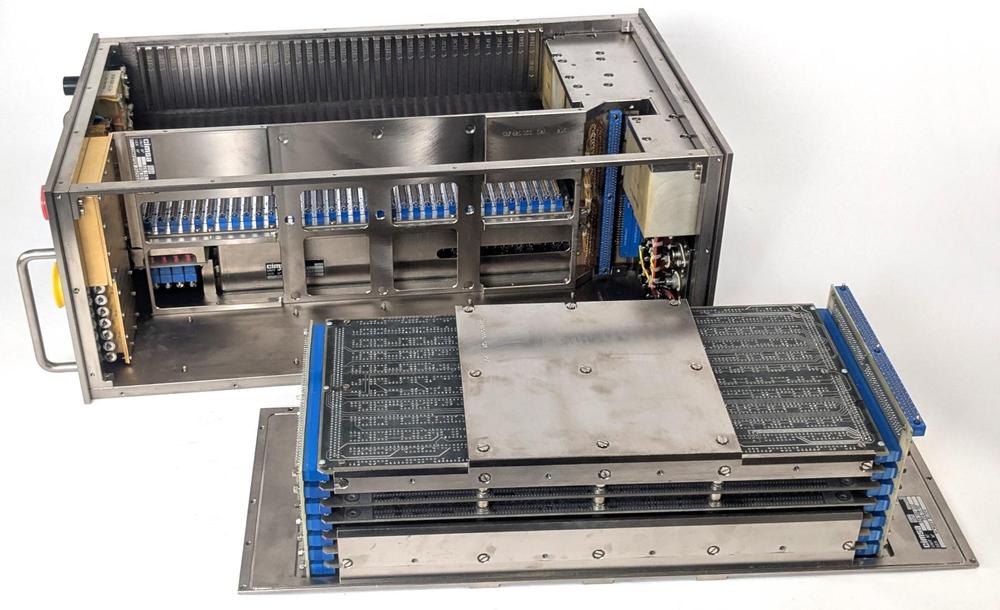
The core memory stack in front of the Mitra computer. The circuit boards have been removed from the far side of the computer.
How core memory works
One of the hardest problems for early computers was storage.
Computers of the late 1940s and early 1950s stored data through techniques such as sound waves in mercury, spots on a CRT screen, or spinning magnetic drums, but these
all had limitations.
What computers needed was dense, inexpensive storage that was fast, reliable, and could be accessed randomly.
During World War II, Germany developed special magnetic alloys that could “flip” from one magnetic state to another.
After the war, American researchers realized that these materials could be used for storing binary data: “It was completely obvious that you could make a
memory with this material,” in the words of Jan Rajchman.
Different aspects of core memory were patented by various inventors (including independent inventor Frederick Viehe, An Wang at Harvard, Jan Rajchman at RCA, and Jay Forrester at MIT), leading to expensive patent battles.
(IBM ended up paying $400,000 to Wang—who used the money to build the computer company Wang Laboratories—and $13,000,000 to MIT.)
I view Jay Forester
as the most important inventor, developing the design of practical core memory, researching magnetic materials, and building the first core memory in 1953 for
the groundbreaking Whirlwind computer.
Core memory is based around a tiny toroidal magnetic core, one per bit.4
A core can be magnetized clockwise or counterclockwise to store a bit.
The core can be magnetized by threading a wire through the core: running a current through the wire produces a magnetic field that magnetizes the core, while
running a current in the opposite direction produces the opposite magnetization.
A key problem with core memory was how to wire the cores without an absurd number of wires: if each core had a separate wire, just 16 KB of storage would require over 100,000 wires.
The solution was called “coincident current addressing”. The cores are arranged in a grid, with horizontal and vertical wires, as shown below.
By running a current through one horizontal wire and one vertical wire, the single core at the intersection was selected.
But wouldn’t that magnetize all the cores along the horizontal and vertical wires?
The key was that the cores were constructed from special magnetic materials with a property called hysteresis: a small current leaves the core completely unchanged,
while a larger current flips the core’s magnetic state.
The currents through the horizontal and vertical wires were carefully selected so each wire had half the current necessary to flip the core; where
the wires intersected, the two currents provided sufficient magnetic field to flip the core.
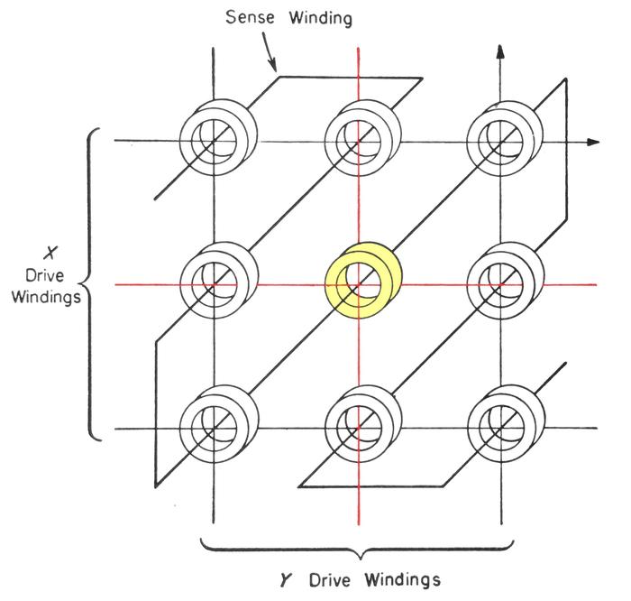
The next step was reading the core.
A sense wire was threaded through all the cores in the two-dimensional plane. To read a core, the X and Y select wires were driven to flip the desired core to the 0 state.
If the core was already in the 0 state, nothing happened. But if the core was originally in the 1 state, the magnetic field changed as the
core changed state. This induced a small current in the sense line, indicating that the core held a 1.
Note that reading the value of a bit destroys that value. Thus, a core needs to be rewritten after reading, to restore the original data.
To access a word of memory at a time, core planes were combined into a three-dimensional stack (below). Since each plane held one bit of the word, a 16-bit word
would have a stack of 16 planes.
All the planes shared the signals to drive the X and Y lines, so a one-word column through the stack was accessed in parallel. Each plane had a separate sense
line to read out the bit.
But how do you write different values to the different bits?
The trick was to put an “inhibit” line through all the cores in a plane, running the inhibit line in the opposite direction to the X lines.
Putting a current through the inhibit line would cancel out the current through the X line, preventing the core in that plane from being modified.
To summarize, a read-write cycle consisted of first energizing a pair of X and Y lines to select a word and write a 0 to the column of cores in that word.
The sense lines provided a readout of the bit values. Next, the X and Y lines were energized in the opposite direction to write a 1 to the cores.
At the same time, the inhibit lines were energized for each plane with a 0 bit. Thus, the cores either flipped back to 1 or stayed at 0, as required.
Many core memories, such as the one below, used a shared wire for sense and inhibit, so there were three wires through each core.
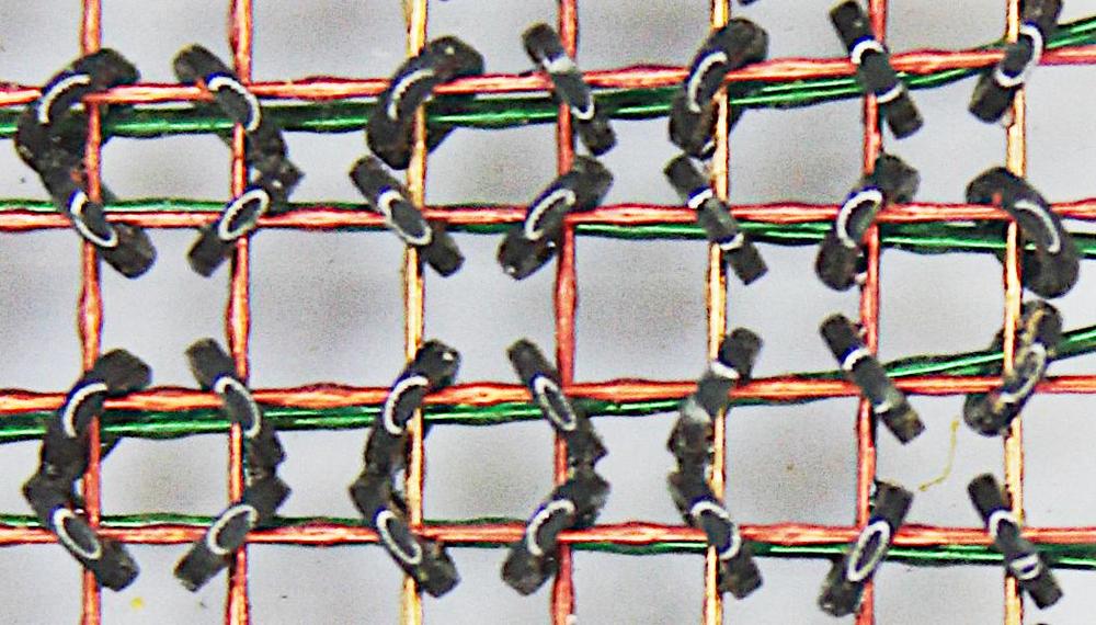
Closeup of an IBM 360 Model 50 core plane. The cores in this computer were called 19-32 because their inner diameter was 19 mils and their outer diameter was 32 mils (0.8 mm).
The final ingredient to make core memory practical was the diode matrix.
The X and Y lines require driver circuits that can produce fast, bidirectional high-current (e.g. 600 mA) pulses.
A core memory plane can have hundreds of these lines. Providing a separate driver for each wire would be very expensive, especially in the vacuum tube era.
The solution was to put separate drivers at each end of the wire, with each driver supporting multiple wires.
For a trivial example, suppose you have 9 vertical lines. Put three drivers (A, B, and C) on the top, each connected to three wires, and three drivers on
the bottom (1, 2, and 3), each connected to three wires.
By energizing a driver at the top and a driver at the bottom (e.g. B and 1), the corresponding wire will be energized. Now, N drivers on each side control N2 wires,
supporting N4 cores in total.
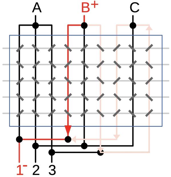
Illustration of how “top” and “bottom” drivers work together to select a single line (red) through the core matrix. However, current can take alternate paths, such as the pink path.
Unfortunately, it’s not quite that easy. Current can take “sneak paths” through the cores, such as the path in pink above.
The solution is to add diodes to ensure that current can’t take the wrong path.
Since a wire needs to be driven with currents in both directions (to flip cores both ways), two diodes are required on each wire, as shown below,
one in each direction.
Each matrix input (A, B, etc.) is replaced with two inputs, one to drive each direction.
(The horizontal wires also require diodes, not shown.)
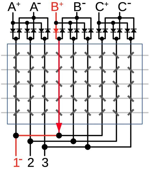
Adding diodes ensures that current only takes the desired path.
Since each wire requires two diodes, core memories used many diodes.
Fortunately, diodes were small and inexpensive, so a large quantity of diodes was manageable. The photo below shows the diode stack
for the computer used in the Saturn V rocket, the Launch Vehicle Digital Computer.
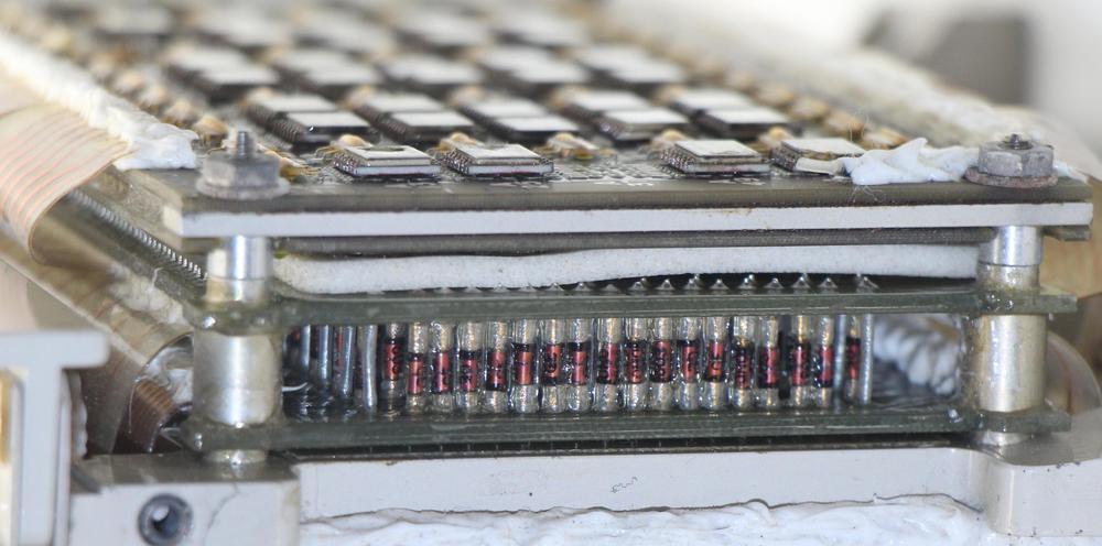
Closeup of the diode matrix in the Saturn V LVDC. Diodes are mounted vertically using cordwood construction between two printed circuit boards.
Originally, core memories were tediously constructed by hand.
For the Whirlwind computer, it took a full 40 hours to wire a 64×64 core plane.
Companies such as IBM soon developed automated techniques to manufacture core memory, and the price dropped by a factor of two every two years, similar
to Moore’s Law.5
Core memories became fast, inexpensive, and reliable, and were the most popular form of main-memory storage until semiconductor memory took over in the 1970s.
The Spacelab computer’s core memory
The Spacelab computer’s memory was manufactured in 1980, a late date for core memory, so it is advanced and high density.
The photo below shows one of the four core plane boards from the computer. Each board holds 16K of 18-bit words (32 KB), so the computer has
128 KB of RAM in total.
The computer is a 16-bit computer, but each word also has a parity bit and a “storage protect” bit, bringing the total to 18 bits.
(The storage protect bit provided write protection on a word-by-word basis, preventing programs from being accidentally overwritten. Because core memory is
nonvolatile, a program could be loaded into memory once and would be immediately available every time the computer was powered on.)
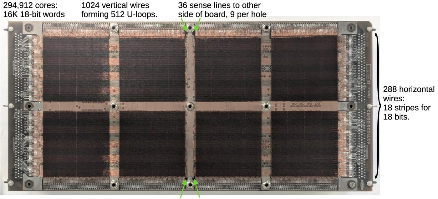
One of the core memory boards from the Spacelab computer.
The core memory board is arranged with 1024 vertical (Y) wires and 288 horizontal (X) wires, supporting 294,912 lithium ferrite cores.
These very thin wires are soldered to tiny pads on the printed-circuit board.
The board supports 18 bits, which is visible as 18 alternating stripes of green and copper because alternating sense lines have different
colors.
The board has 36 sense lines:
the left and right halves of the board have independent sense lines to reduce noise, so the board has 36 sense lines for 18 bits.
The sense wires pass through four holes in the board (green arrows) and are soldered on the back of the board.
The photo below shows a close-up of the cores.
Each core is approximately 32 mils (0.8mm) in diameter, the same as the IBM System/360 cores shown earlier. However, the cores are stacked much closer, with
only a small gap between cores.
The X and Y select lines are copper-colored, while the sense lines are green. (The wires are all enameled to prevent short circuits.)
The sense wires loop around at the left, forming a single circuit through each bit section.
Half the Y lines form loops at the bottom; the other half form loops at the top. Thus, each Y line passes through the plane twice in a U-shaped path, which will
turn out to be important.
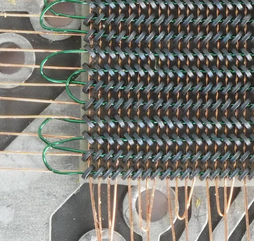
A close-up of the cores. I think that some rows tilt left and some tilt right to ensure that the sense lines keep the same polarity when they switch direction. Photo courtesy of CuriousMarc.
The other side of each circuit board holds the sense amplifiers and the diode matrix for the core plane.
The diode chips are the square black packages, each containing 16 diodes for 8 core lines.6
In the red-outlined regions, one end of each vertical U-loop is connected to a diode chip; the lines of diagonal holes are the vias that pass each signal
through the board.
The other end of each vertical U-loop is connected to one of the blue board connectors on the side; these vias are in the blue-outlined regions.
The horizontal lines use the diode chips and vias in the green regions.
One end of each line is connected to a diode chip, while the other end is connected to a board connector through traces on the other side.
Note that some vertical lines connect to the diode chips at the top of the board, while others connect at the bottom.
Similarly, some horizontal lines connect at the left while others connect at the right.
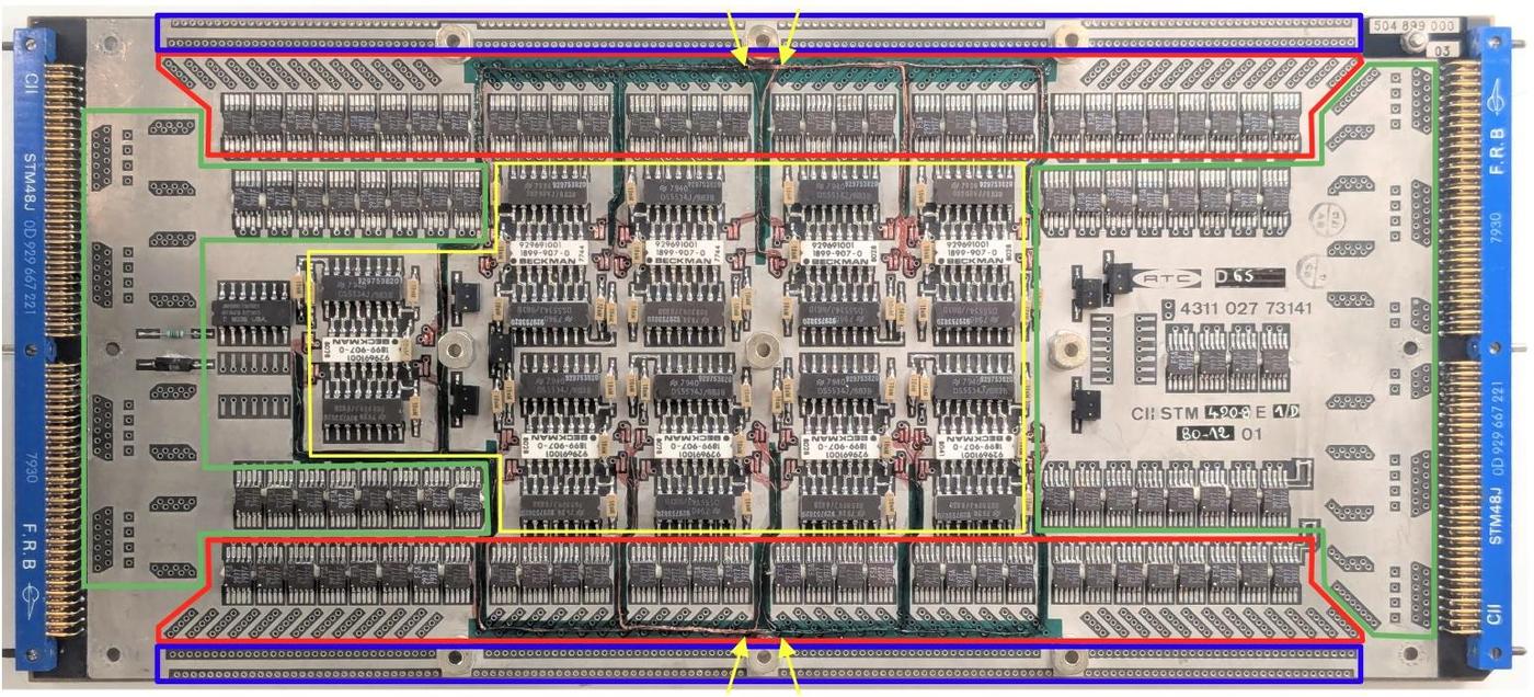
The back side of the core plane board holds the diode matrices and sense amplifiers.
The central region (yellow) holds 18 sense amplifier chips, the black DIP integrated circuits, each containing two amplifiers.7
The white packages are resistor packages, holding multiple resistors to bias and terminate the sense amplifier lines.
The wires from the sense amplifiers are connected as twisted pairs that are soldered to the board right next to the corresponding sense amplifier
chips.
Using twisted pairs for the whole distance prevents the wires from picking up electrical noise, which could overwhelm the tiny signals in the sense wires.
The sense wires pass from one side of the board to the other through four holes in the board (yellow arrows), and then are glued down as they traverse a significant distance
on the board.
(It must have been difficult to manufacture the board without breaking the tiny, fragile wires.)
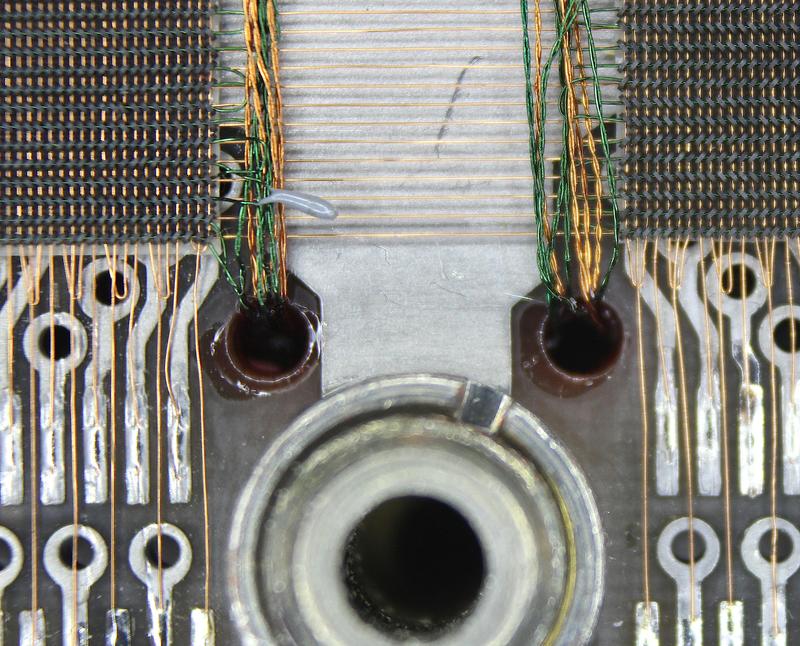
Each sense wire loop forms a twisted pair that is fed to the other side through a hole in the circuit board. Above the hole, you can see a gray blob where
sense wires were spliced for some reason.
Also note how alternating vertical wires are soldered to the
circuit board, with circular vias connected to the other side. The other vertical wires form loops.
are soldered to the circuit board
Detecting signals on the sense lines is tricky because the pulses are very small, a few millivolts.
Because the sense lines run next to the X drive lines, they can easily pick up noise from the high-current pulses on the X lines.
To minimize this noise,
the sense lines cross each other between two plane sections, forming a “bow tie”, as shown below.
The result is that an X line runs next to the positive sense line for half the length and the negative sense line for the other half. Thus,
the induced noise cancels out.
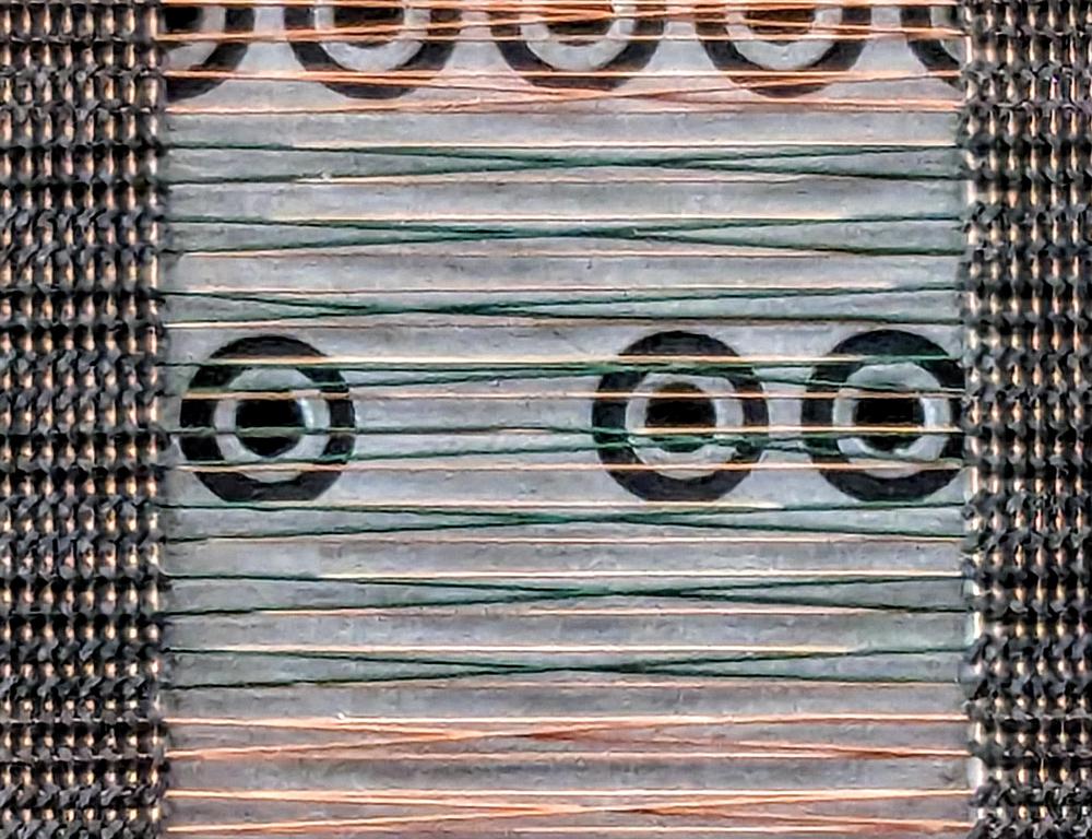
A close-up of the sense lines. The 16 sense lines in the middle are green, while the sense lines above and below (as well as the X lines) are copper. Note that the sense lines cross, while the X lines continue horizontally. The large circles are vias through the board.
The core memory in the Spacelab computer used a different architecture from a typical core memory, improving performance by eliminating the inhibit line.
This architecture was called a 2½D memory.8
If you’re familiar with core memory, the lack of inhibit lines may seem puzzling: how do you write 1 to some bits and 0 to other bits?
The trick is to have separate X driver circuitry for each bit.9
When writing data, the X lines are only energized for bits that receive a 1; the other lines are left unenergized, so the bits remain at 0.
The disadvantage is that instead of one set of X driver circuits, you now need one set for each bit, a factor of 18 more for an 18-bit word.
However, with the development of core drivers on integrated circuits, the cost of the additional driver circuitry became less significant.
The memory system used an technique called phase reversal to cut the number of vertical drivers in half.
Recall that pairs of vertical wires are joined by a U-connection.
By driving the wire in a particular direction, the left side or the right side of the pair can be selected.
For example, the drawing below shows how the two wires select the left core, but not the right core. In the left core, both currents go through the core in the same direction, inducing a magnetic field in the toroid.10
But in the right core, the two currents cancel out, so there is no magnetic field created.
But if the current in the vertical loop is reversed, the right core will be selected, rather than the left core.
The point is that instead of using two drivers for the vertical wires, one driver is used, reversing the current to select the left or right core.
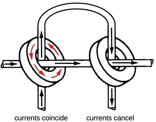
Connecting pairs of vertical wires into a U-shaped loop lets each driver control twice as many cores.
The diagram below shows the complex wiring for X drive wires.
Each band of 16 wires corresponds to one bit in the 18-bit word, and has a separate sense wire.
The top band of 16 X lines is connected to four contacts on the board connector; each contact is connected to four X lines through the curving PCB traces.
The bottom band of 16 X lines is wired to diode modules on the other side of the board, connected through the round vias.
(Each wire has the opposite connections—diode module or board connector—on the other end.)11
One group of four X wires is energized through the connector, while four wires are energized through the diode matrix, selecting one of the 16 X wires in the group.
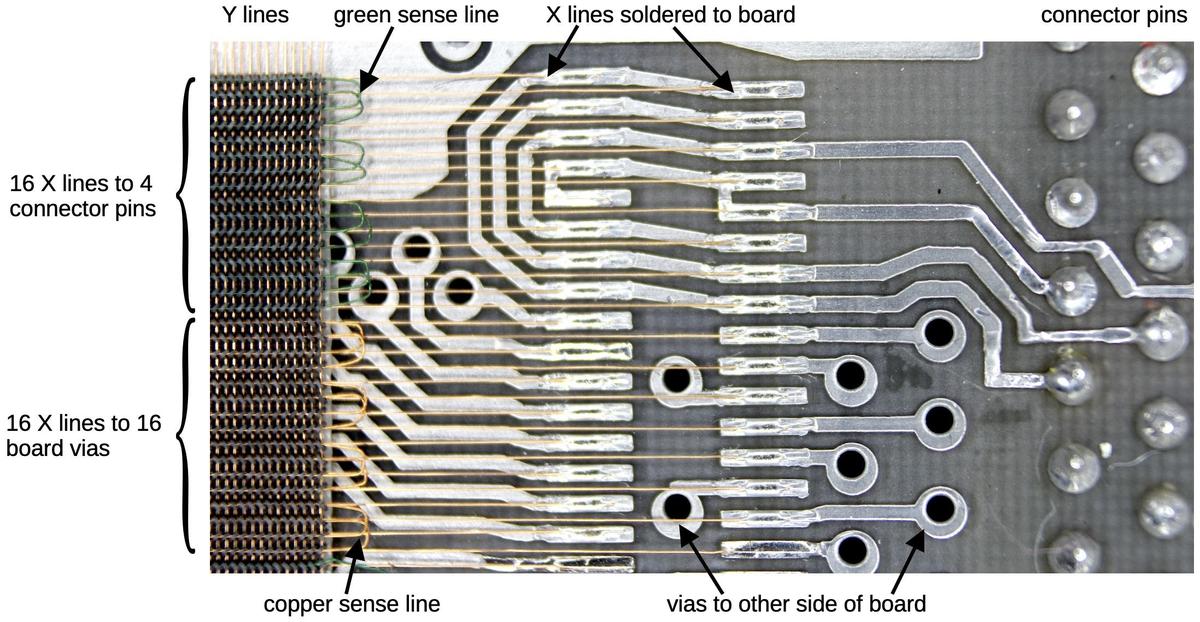
The PCB wiring for the X lines.
Other boards in the memory stack
The memory stack has seven boards in total, arranged as a driver board, the four core planes, a second driver board, and an interface board.
I haven’t examined these boards in detail, but I’ll give some preliminary information.
The photo below shows one of the two driver boards.
It provides the high-current pulses for the X and Y select lines.
The board is crammed with specialized core memory driver chips12, along with a few logic chips to control the drivers.
It has separate drivers for the two ends of the select lines, allowing the matrix selection described earlier.
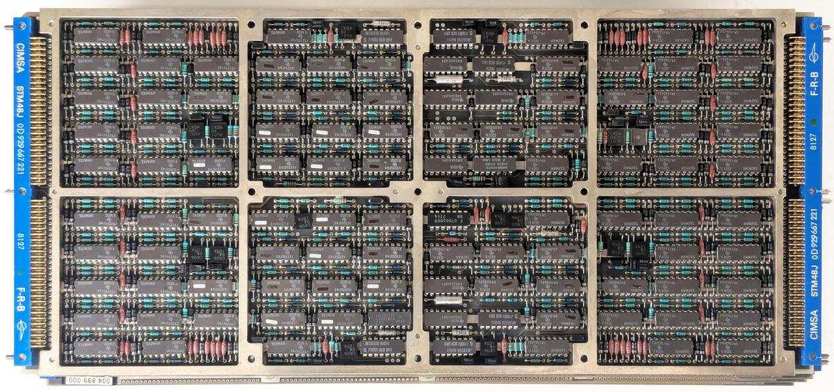
One of the two memory driver boards. Click this image (or any other) for a larger version.
Since there are two driver boards and four core memory boards, at first I thought that each driver board controlled two core memory boards.
The configuration turns out to be more complicated, with one more layer of matrix selections to cut the number of drivers in half.
To simplify slightly, consider the X lines on a core board to have left ends and right ends, both of which must be energized to activate a line.
For the left ends, the first driver board powers core boards 1 and 2, while the second driver board powers core boards 3 and 4.
The right ends are shuffled: the first driver board powers core boards 1 and 3, while the second driver board powers core boards 2 and 4.
Now, if the first driver board powers the left and right ends, core board 1 is the only one with both ends active.
If the first driver board powers the left ends while the second board powers the right ends, core board 2 is activated.
Similarly, core board 3 or 4 can be activated.
The point is that since each set of drivers is connected to two core boards, two sets of drivers are required instead of four.
The final board is the interface to the rest of the computer.
It has many transistor arrays in DIP packages, along with many resistors.
It seems that the board uses discrete transistors to drive the bus, rather than using interface chips, which is unexpected.
The board has some wire-wrapped jumpers in the lower center region, presumably for configuration.
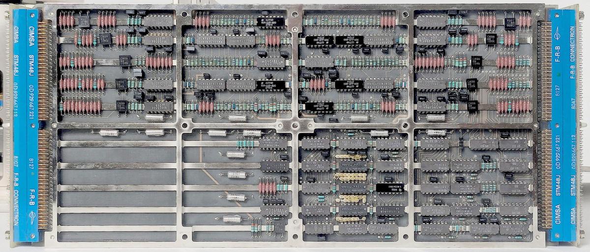
The interface board has some unused space in the lower left.
Conclusions
Core memory had a long life, surviving even as computers migrated from vacuum tubes to transistors and then integrated circuits, but eventually
semiconductor memory made it obsolete.13
Core memories lasted even longer in aerospace applications since it had two key advantages over semiconductor memory: it retained data even without power, and it was resistant to radiation.
The Spacelab computer, manufactured in 1980, was near the end of core memory’s reign, so it is more advanced than a typical core memory system, with
higher density, extensive use of integrated circuits, and the 2½D architecture.
But eventually the high density, low cost, and low power consumption of semiconductor memory won out.
In 1991, the Space Shuttle flew with upgraded main computers, the IBM AP-101S that used semiconductor memory instead of magnetic core.
Spacelab’s Mitra computers were also replaced, using the AP-101SL, which was based on the AP-101S but modified to support
the instruction set and peripherals of the original Spacelab computer.14
Although core memory is now firmly in the past, it still lives on in the expression “core dump”.
I plan to investigate the Spacelab computer some more.
For updates, follow me on
Bluesky (@righto.com),
Mastodon (@[email protected]),
or RSS.
Credits: Thanks to Steve Jurvetson for providing the Spacelab computer. Thanks to CuriousMarc for photography and help disassembling the computer.
AI statement: Despite the presence of the em dash, no AI was used in the writing of this article (details).
Notes and references
💬 **What’s your take?**
Share your thoughts in the comments below!
#️⃣ **#core #memory #module #Spacelab #computer**
🕒 **Posted on**: 1788121375
🌟 **Want more?** Click here for more info! 🌟
