🔥 Explore this awesome post from Hacker News 📖
📂 **Category**:
✅ **What You’ll Learn**:

What is “real”? How do you define “real”? If you’re talking about what you can feel, what you can smell, taste, and see… then “real” is simply electrical signals interpreted by your brain.
— Morpheus, The Matrix
If the processor is the brain of the computer, could it also be part of some kind of virtual reality? Simulated memory, software-defined peripherals, artificially generated interrupts.
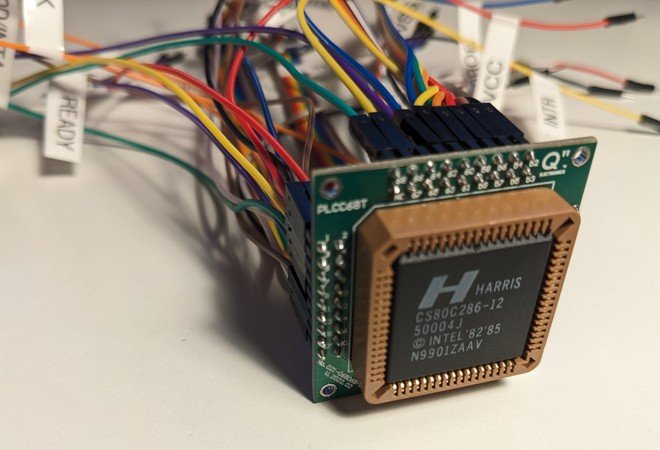
My first computer was a 286 with 1 MB of RAM and a 50 MB HDD (if I remember correctly). So I decided to pick up a 286 processor and try to simulate the rest of the computer around it. Or at least make it to boot up and run some simple assembly code.
Two years ago, I ordered two (that’s how many came in a package) Harris 80C286-12 processors. My memories are a bit hazy, but I believe the C in its name is important because these are the types that are less sensitive to clock accuracy (the 12 at the end means it likes to run at 12 MHz), and can even be stepped manually.
At first, I wasn’t too successful with it, and the project ended up in a drawer. Then this year, I picked it up again and tried to figure out where things went wrong.
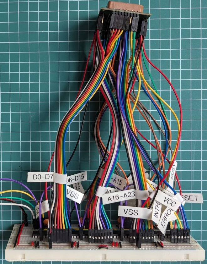
Wiring up
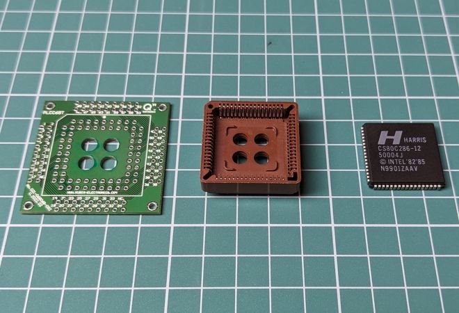
The processor fits into a PLCC-68 socket. The pins of the socket are not suitable for plugging in jumper wires directly, so the socket was mounted onto an adapter PCB with jumper-compatible headers. The pinout of both the chip and the socket is included in the datasheet, but the adapter PCB complicates things a bit, so I created a small conversion table to make my life easier.
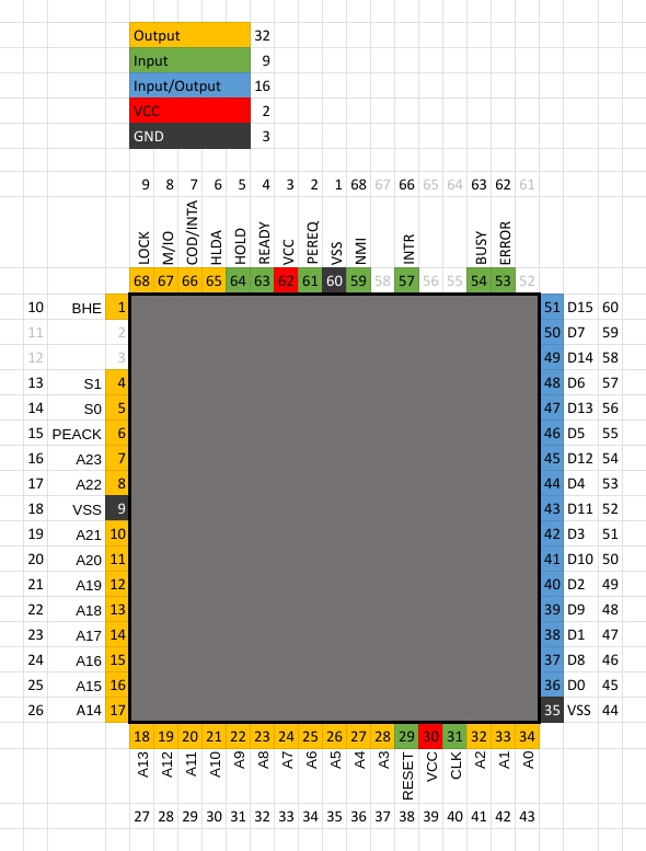
The table also helped identify the various inputs and outputs, which would later be useful when connecting to the Raspberry Pi. As you can see, no fewer than 57 pins are required, which is more than the Pi can provide. The MCP23S17 IO expander came to the rescue. While it wouldn’t allow us to drive the processor at the breakneck speed of the supported 12 MHz, fortunately, that’s not our goal.
The chip contains 16 IO pins, so we’ll need four of them. Although each pin can individually be configured as input or output, I tried to group them logically. The expander has side A and side B, each with 8 pins, and the final result looked like this:
         ┌───┬──┬───┐
         ┤   └──┘   ├
         ┤          ├
         ┤   FLAG   ├ ERROR
         ┤          ├ BUSY
         ┤ ADDR:100 ├ INTR
   READY ┤          ├ NMI
   RESET ┤B        A├ PEREQ
     CLK ┤          ├ HOLD
         └──────────┘
         ┌───┬──┬───┐
    HLDA ┤   └──┘   ├ A23
COD/INTA ┤          ├ A22
    M/IO ┤   MISC   ├ A21
    LOCK ┤          ├ A20
     BHE ┤ ADDR:011 ├ A19
      S1 ┤          ├ A18
      S0 ┤B        A├ A17
   PEACK ┤          ├ A16
         └──────────┘
         ┌───┬──┬───┐
      A8 ┤   └──┘   ├ A7
      A9 ┤          ├ A6
     A10 ┤   ADDR   ├ A5
     A11 ┤          ├ A4
     A12 ┤ ADDR:010 ├ A3
     A13 ┤          ├ A2
     A14 ┤B        A├ A1
     A15 ┤          ├ A0
         └──────────┘
         ┌───┬──┬───┐
      D8 ┤   └──┘   ├ D7
      D9 ┤          ├ D6
     D10 ┤   DATA   ├ D5
     D11 ┤          ├ D4
     D12 ┤ ADDR:001 ├ D3
     D13 ┤          ├ D2
     D14 ┤B        A├ D1
     D15 ┤          ├ D0
         └──────────┘
The Pi communicates with the expanders over SPI. Several solutions exist for this. I chose the one where all chips are active simultaneously, and the Pi is sending them messages by their hardware address.
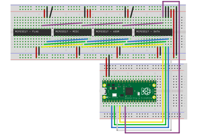
The RESET pin (wired with the purple cable) does not need to be controlled by the Pi in this case, but during one of the debugging sessions, I tried it in the hopes that it would help, and it remained that way. Now we just need to connect everything with a truckload of jumper wires, and we could move on to programming.
IO Expansion
We only need a relatively small portion of the MCP23S17’s capabilities. We just have to configure the direction of the IO pins and read/write the relevant registers. Configuration is done by modifying register values. First, we need to enable the use of hardware addressing. By default, all chips have the address 000, so if we send a register modification to that address (setting the HAEN bit in the IOCON register), hardware addressing will be enabled simultaneously on all four chips.
After a few hours (days) of head-scratching, it turned out that this alone is not necessarily sufficient for proper operation. We also need to send the same message to the configured hardware address itself to enable hardware addressing (rather odd, I know). So if, for example, we set the hardware address to 101, we must resend the original register modification message previously sent to 000 to 101 as well.
Now that hardware addressing is sorted out, we need to set the IODIRA and IODIRB registers of each chip to the appropriate direction. Because of our grouping, we can configure an entire side at once for reading (11111111) or writing (00000000). Further details can be found in the chip’s datasheet.
Originally, I started working with a Pi Zero, but eventually settled on a Pi Pico running MicroPython. To manage the expander chips, I created the following small class:
class MCP23S17:
    IODIRA = 0x00
    IODIRB = 0x01
    IOCON = 0x0B
    GPIOA = 0x12
    GPIOB = 0x13

    def __init__(self, address, spi, cs):
        self.__address = address
        self.__spi = spi
        self.__cs = cs

    def init(self):
        self.__writeRegister(0b01000000, self.IOCON, 0b00001000)
        self.writeRegister(self.IOCON, 0b00001000)

    def writeRegister(self, reg, value):
        self.__writeRegister(self.__address, reg, value)

    def readRegister(self, reg):
        tx = bytearray([self.__address | 1, reg, 0])
        rx = bytearray(3)
        self.__cs.value(0)
        self.__spi.write_readinto(tx, rx)
        self.__cs.value(1)
        return rx[2]

    def __writeRegister(self, address, reg, value):
        self.__cs.value(0)
        self.__spi.write(bytes([address, reg, value]))
        self.__cs.value(1)
In init, you can clearly see that we set the value of the IOCON register twice. We can use the class as follows to communicate with the processor:
spi = SPI(0, baudrate=1000000, sck=Pin(2), mosi=Pin(3), miso=Pin(4))
cs = Pin(5, mode=Pin.OUT, value=1)
rst = Pin(6, mode=Pin.OUT, value=0)

chip_data = MCP23S17(0b01000010, spi, cs)
chip_addr = MCP23S17(0b01000100, spi, cs)
chip_misc = MCP23S17(0b01000110, spi, cs)
chip_flag = MCP23S17(0b01001000, spi, cs)

rst.value(1)

chip_data.init()
chip_addr.init()
chip_misc.init()
chip_flag.init()

chip_data.writeRegister(MCP23S17.IODIRA, 0xff)
chip_data.writeRegister(MCP23S17.IODIRB, 0xff)

chip_addr.writeRegister(MCP23S17.IODIRA, 0xff)
chip_addr.writeRegister(MCP23S17.IODIRB, 0xff)

chip_misc.writeRegister(MCP23S17.IODIRA, 0xff)
chip_misc.writeRegister(MCP23S17.IODIRB, 0xff)

chip_flag.writeRegister(MCP23S17.IODIRA, 0x00)
chip_flag.writeRegister(MCP23S17.IODIRB, 0x00)
At first, I missed the init calls here and was surprised when nothing worked. Most of the pins are configured for reading; only the flags need to be set to writing.
The Initial State
Before we can do anything, we need to RESET the processor. For this, the RESET flag must be held active for at least 16 clock cycles, and switching it on and off must be synchronized with the clock flag. First, I created a few constants for the flags to make life easier:
FLAG_ERROR = 0x20
FLAG_BUSY  = 0x10
FLAG_INTR  = 0x08
FLAG_NMI   = 0x04
FLAG_PEREQ = 0x02
FLAG_HOLD  = 0x01


FLAG_CLK   = 0x80
FLAG_RESET = 0x40
FLAG_READY = 0x20


FLAG_PEACK    = 0x80
FLAG_S0       = 0x40
FLAG_S1       = 0x20
FLAG_BHE      = 0x10
FLAG_LOCK     = 0x08
FLAG_M_IO     = 0x04
FLAG_COD_INTA = 0x02
FLAG_HLDA     = 0x01
It’s worth comparing this with the earlier MCP23S17 pin mapping. We treat each group of 8 pins as 8 bits / 1 byte of data. For example, in the byte from the ‘misc’ chip’s GPIOB side, the HLDA flag is the least significant bit, while PEACK is the most significant.
PEACK
↓
10100111
       ↑
    HLDA
With the flags in place, we can perform the RESET:
for i in range(17):
    chip_flag.writeRegister(MCP23S17.GPIOB, FLAG_CLK | FLAG_RESET)
    time.sleep(0.001)
    chip_flag.writeRegister(MCP23S17.GPIOB, FLAG_RESET)
    time.sleep(0.001)
The sleep intervals were chosen more or less arbitrarily; we don’t have to adhere to any strict timing. During RESET, the processor must enter a defined state. We can verify this with the following piece of code:
data = chip_addr.readRegister(MCP23S17.GPIOA)
print('A7-0:   ' + str(bin(data)))
data = chip_addr.readRegister(MCP23S17.GPIOB)
print('A15-8:  ' + str(bin(data)))
data = chip_misc.readRegister(MCP23S17.GPIOA)
print('A23-16: ' + str(bin(data)))
data = chip_misc.readRegister(MCP23S17.GPIOB)
print('PEACK, S0, S1, BHE, LOCK, M/IO, COD/INTA, HLDA: ' + str(bin(data)))
The values we expect to see look like this:
A7-0:   0b11111111
A15-8:  0b11111111
A23-16: 0b11111111
PEACK, S0, S1, BHE, LOCK, M/IO, COD/INTA, HLDA: 0b11111000
Strangely enough, I was greeted with the following instead:
A7-0:   0b11111111
A15-8:  0b11111000
A23-16: 0b11111111
PEACK, S0, S1, BHE, LOCK, M/IO, COD/INTA, HLDA: 0b11111000
It was hard not to notice that the values in the second and fourth lines were identical. I checked all the connections, disassembled everything, debugged with LEDs to ensure the values I wrote were going to the right places, replaced the chip assigned to the A15-8 pins, swapped the processor for the spare, reread the code a thousand times, but nothing helped.
Then I found that hardware addressing trick mentioned earlier with the MCP23S17, and everything started to work like magic. The point is, if everything went well, we can release the RESET flag, and the boot process can begin.
chip_flag.writeRegister(MCP23S17.GPIOB, FLAG_CLK | FLAG_RESET)
time.sleep(0.001)
chip_flag.writeRegister(MCP23S17.GPIOB, 0)
time.sleep(0.001)
Initialization
After this, within 50 clock cycles, the processor must begin to read the first instruction to execute from address 0xFFFFF0. The COD/INTA, M/IO, S0, and S1 flags determine what the processor intends to do.
COD/INTA |
M/IO |
S0 |
S1 |
Bus cycle |
|---|---|---|---|---|
| 0 | 0 | 0 | 0 | Interrupt acknowledge |
| 0 | 1 | 0 | 0 | halt / shutdown |
| 0 | 1 | 0 | 1 | Memory data read |
| 0 | 1 | 1 | 0 | Memory data write |
| 1 | 0 | 0 | 1 | I/O read |
| 1 | 0 | 1 | 0 | I/O write |
| 1 | 1 | 0 | 1 | Memory instruction read |
I left out the less interesting ones from the table; they can be viewed in the datasheet. For our small test, we’ll only need these four:
- halt / shutdown
- memory data write
- memory data read
- memory instruction read
So we start sending clock signals and wait until we reach the first ‘Memory instruction read’:
cycle = 1
while True:
    print(f'#💬')
    chip_flag.writeRegister(MCP23S17.GPIOB, FLAG_CLK)
    time.sleep(0.001)
    chip_flag.writeRegister(MCP23S17.GPIOB, 0)
    time.sleep(0.001)

    data = chip_misc.readRegister(MCP23S17.GPIOB)
    PEACK = data & FLAG_PEACK
    S0 = data & FLAG_S0
    S1 = data & FLAG_S1
    BHE = data & FLAG_BHE
    LOCK = data & FLAG_LOCK
    M_IO = data & FLAG_M_IO
    COD_INTA = data & FLAG_COD_INTA
    HLDA = data & FLAG_HLDA

    if not COD_INTA and M_IO and not S1 and not S0:
        print('halt / shutdown')
        sys.exit(0)
    elif not COD_INTA and M_IO and not S1 and S0:
        print('Memory data read')
    elif not COD_INTA and M_IO and S1 and not S0:
        print('Memory data write')
    elif COD_INTA and M_IO and not S1 and S0:
        print('Memory instruction read')

    time.sleep(0.01)
    cycle += 1
When we arrive successfully, we can start sending, say, NOP (0x90) instructions. We set the data bus to write mode, put the NOP instruction on it, send a clock signal, then set the data bus back to read mode.
chip_data.writeRegister(MCP23S17.IODIRA, 0x00)
chip_data.writeRegister(MCP23S17.IODIRB, 0x00)
chip_data.writeRegister(MCP23S17.GPIOA, 0x90)
chip_data.writeRegister(MCP23S17.GPIOB, 0x90)

chip_flag.writeRegister(MCP23S17.GPIOB, FLAG_CLK)
time.sleep(0.001)
chip_flag.writeRegister(MCP23S17.GPIOB, 0)
time.sleep(0.001)

chip_data.writeRegister(MCP23S17.IODIRA, 0xFF)
chip_data.writeRegister(MCP23S17.IODIRB, 0xFF)
Complex Mathematical Operations
That’s all well and good, but let’s look at something more interesting. Something that requires both reading and writing memory. A simple little program that reads two numbers from memory, adds them, and writes the result back to memory.
Since we start very close to the end of memory (0xFFFFF0), we don’t have much room, so first we need to jump elsewhere.
reset.asm
[cpu 286]
org 0xfff0

jmp 0x0000:0x0500
Then comes the addition:
add.asm
[cpu 286]
org 0x0500

xor  ax, ax
mov  ds, ax

mov  ax, [num1]
add  ax, [num2]
mov  [result], ax

hlt


num1    dw 0x1234
num2    dw 0x000a
result  dw 0x0000
Using the nasm program, we can also generate a binary from it:
$ nasm reset.asm
$ nasm add.asm
Then, with a short Python script, we can convert it into a Python-friendly format so we can load it into our virtual memory:
hex_dump.py
import sys

with open(sys.argv[1], "rb") as f:
    data = f.read()
hex_values = ", ".join(f"0x⚡" for byte in data)
print(f"[🔥]")
$ python hex_dump.py reset
[0xea, 0x00, 0x05, 0x00, 0x00]
$ python hex_dump.py add
[0x31, 0xc0, 0x8e, 0xd8, 0xa1, 0x0f, 0x05, 0x03, 0x06, 0x11, 0x05, 0xa3, 0x13, 0x05, 0xf4, 0x34, 0x12, 0x0a, 0x00, 0x00, 0x00]
To simulate memory, I put together the following small class:
class Memory:
    def __init__(self):
        self.__data = ⚡

    def load(self, base, data):
        for i, b in enumerate(data):
            self.__data[base + i] = b

    def __getitem__(self, address):
        return self.__data.get(address, 0x00)

    def __setitem__(self, address, value):
        self.__data[address] = value & 0xFF
It’s just a simple dict with a helper function that allows us to load data into arbitrary addresses. Which we then do with the code generated by nasm:
MEMORY = Memory()
MEMORY.load(0x000500, [
    0x31, 0xc0,
    0x8e, 0xd8,
    0xa1, 0x0f, 0x05,
    0x03, 0x06, 0x11, 0x05,
    0xa3, 0x13, 0x05,
    0xf4,
    0x34, 0x12,
    0x0a, 0x00,
    0x00, 0x00
])
MEMORY.load(0xfffff0, [
    0xea, 0x00, 0x05, 0x00, 0x00
])
All that remains is to handle the cases. But first, we need to talk about the BHE flag and the A0 pin.
BHE |
A0 |
Function |
|---|---|---|
| 0 | 0 | Word transfer |
| 0 | 1 | Byte transfer on upper half of data bus (D15 – D8) |
| 1 | 0 | Byte transfer on lower half of data bus (D7 – D0) |
So during an operation involving the data bus, we can read/write the entire data bus, its upper half, or its lower half.
In our case, ‘Memory data read’ is very similar to ‘Memory instruction read’, so we can handle both with the same code. We just need to handle the flags mentioned above and use the fake memory.
address = (a3 << 16) + (a2 << 8) + a1
if not COD_INTA and M_IO and not S1 and S0:
    print('Memory data read 0x{:06X}'.format(address))
else:
    print('Memory instruction read 0x{:06X}'.format(address))

if not BHE and not A0:
    print('Word transfer 0x{:02X}{:02X}'.format(MEMORY[address + 1], MEMORY[address]))
    chip_data.writeRegister(MCP23S17.IODIRA, 0x00)
    chip_data.writeRegister(MCP23S17.IODIRB, 0x00)
    chip_data.writeRegister(MCP23S17.GPIOA, MEMORY[address])
    chip_data.writeRegister(MCP23S17.GPIOB, MEMORY[address + 1])
elif not BHE and A0:
    print('Byte transfer on upper half of data bus 0x{:02X}'.format(MEMORY[address]))
    chip_data.writeRegister(MCP23S17.IODIRB, 0x00)
    chip_data.writeRegister(MCP23S17.GPIOB, MEMORY[address])
elif BHE and not A0:
    print('Byte transfer on lower half of data bus 0x{:02X}'.format(MEMORY[address]))
    chip_data.writeRegister(MCP23S17.IODIRA, 0x00)
    chip_data.writeRegister(MCP23S17.GPIOA, MEMORY[address])

chip_flag.writeRegister(MCP23S17.GPIOB, FLAG_CLK)
time.sleep(0.001)
chip_flag.writeRegister(MCP23S17.GPIOB, 0)
time.sleep(0.001)

chip_data.writeRegister(MCP23S17.IODIRA, 0xFF)
chip_data.writeRegister(MCP23S17.IODIRB, 0xFF)
It’s not much more complicated than our original NOP-based solution, but there is an extra twist here that’s easy to stumble over. In what order should we place the bytes onto the data bus? The GPIOA register represents the least significant byte of the data bus, while GPIOB represents the most significant. So, for example, our initial JMP instruction (0xea00) will travel as 0x00ea (little-endian).
It’s worth scrolling back a bit and noticing that nasm already performed similar swaps. For instance, our 0x1234 value used for the addition is stored in memory as 0x3412.
‘Memory data write’ is very straightforward; we simply use the fake memory:
address = (a3 << 16) + (a2 << 8) + a1
print('Memory data write 0x{:06X}'.format(address))

if not BHE and not A0:
    print('Word transfer 0x{:02X}{:02X}'.format(d2, d1))
    MEMORY[address] = d1
    MEMORY[address + 1] = d2
elif not BHE and A0:
    print('Byte transfer on upper half of data bus 0x{:02X}'.format(d2))
    MEMORY[address] = d2
elif BHE and not A0:
    print('Byte transfer on lower half of data bus 0x{:02X}'.format(d1))
    MEMORY[address] = d1
The little-endian order can also be observed here, although during execution, I didn’t encounter a case where it attempted to write two bytes to memory at once.
And during ‘halt / shutdown’, we simply print the result of the addition from memory and exit:
print('Result: 0x{:04X}'.format((MEMORY[0x000514] << 8) + MEMORY[0x000513]))
sys.exit(0)
The Final Result
In the end, running the program should produce output similar to this, where you can see it reading the initial JMP instruction, jumping to the new address, continuing to read instructions from there, reading the two numbers to be added from memory, and finally writing the result back to memory:
RESET
A7-0:   0b11111111
A15-8:  0b11111111
A23-16: 0b11111111
PEACK, S0, S1, BHE, LOCK, M/IO, COD/INTA, HLDA: 0b11111000
START
#40
Memory instruction read 0xFFFFF0
Word transfer 0x00EA
#43
Memory instruction read 0xFFFFF2
Word transfer 0x0005
#46
Memory instruction read 0xFFFFF4
Word transfer 0x0000
#49
Memory instruction read 0xFFFFF6
Word transfer 0x0000
#52
Memory instruction read 0xFFFFF8
Word transfer 0x0000
#67
Memory instruction read 0x000500
Word transfer 0xC031
#70
Memory instruction read 0x000502
Word transfer 0xD88E
#73
Memory instruction read 0x000504
Word transfer 0x0FA1
#76
Memory instruction read 0x000506
Word transfer 0x0305
#79
Memory instruction read 0x000508
Word transfer 0x1106
#82
Memory instruction read 0x00050A
Word transfer 0xA305
#85
Memory instruction read 0x00050C
Word transfer 0x0513
#88
Memory data read 0x00050F
Byte transfer on upper half of data bus 0x34
#91
Memory data read 0x000510
Byte transfer on lower half of data bus 0x12
#94
Memory instruction read 0x00050E
Word transfer 0x34F4
#99
Memory data read 0x000511
Byte transfer on upper half of data bus 0x0A
#102
Memory data read 0x000512
Byte transfer on lower half of data bus 0x00
#115
Memory data write 0x000513
Byte transfer on upper half of data bus 0x0A
#116
Memory data write 0x000513
Byte transfer on upper half of data bus 0x3E
#119
Memory data write 0x000514
Byte transfer on lower half of data bus 0x12
#120
Memory data write 0x000514
Byte transfer on lower half of data bus 0x12
#123
halt
Result: 0x123E
It was a tremendous joy to see the correct final result at the end of execution for the first time. I think I’ve reached a milestone where I can stop and take a rest for now.
Of course, we’ve only scratched the surface; there’s still a great deal left to learn. It’s worth going through the processor’s datasheet, or perhaps thinking about how various peripherals (such as a keyboard or a text display) are actually implemented.
What is certain, however, is that for the processor, this reality is not virtual at all. It doesn’t matter to it where the electrical signals are coming from, as long as they are compatible with its own internal reality.
{💬|⚡|🔥} **What’s your take?**
Share your thoughts in the comments below!
#️⃣ **#Computergenerated #dream #world #deadlime**
🕒 **Posted on**: 1772429374
🌟 **Want more?** Click here for more info! 🌟