🔥 Explore this must-read post from Hacker News 📖
📂 Category:
📌 Main takeaway:
In this article we’re going to take a look at how to reverse-engineer
vintage synthesiser firmware. The synthesiser I’ve chosen for us to
look at is the Yamaha DX7 (See Appendix: Why Choose This Synth?). You don’t need a DX7 to follow along at home, but you will need a
copy of the DX7 V1.8 firmware (available
here) and the
Ghidra
disassembler.
Who is this article for?
This article’s intended audience is people from a technical
background who are new to reverse-engineering, 8-bit architectures,
or embedded development. If you come from an electrical-engineering
or embedded-software background, you’ll probably find the content
here a little basic.
You’ll only need to know a little bit about low-level programming: A
basic understanding of how binary and pointers work should be
enough. You don’t need to know assembly language, or understand any
specific processor architecture.
A few years ago I decided to give myself a crash course on what goes
on inside synthesisers. I ended up writing the article
Yamaha DX7 Technical Analysis
about what I’d learned. In order to tease out some more details about
the DX7’s inner-workings, I decided to
disassemble the synth’s firmware ROM. I didn’t have any experience with reverse-engineering binaries, so
I had to figure it out as I went. I’m still by no means an expert (if you see any mistakes in this article, please let me know!), but I’d like to share what I’ve learned.
All I had when I started was a copy of the firmware, a copy of the
service manual, and a can-do attitude. I knew nothing about
8-bit systems, and absolutely nothing about electronics, but
I was willing to give anything a shot. If this sounds like you, read
on, and I hope you find this article helpful!
Reverse-engineering vintage synthesisers is a great introduction to
embedded systems, and can be a lot of fun. In a lot of ways
reverse-engineering is a bit like putting together a big jigsaw
puzzle. Sometimes putting a new piece in place unlocks a lot of new
progress, and like a jigsaw puzzle, the best place to start is at the
edges.
Address Decoding #
The peripheral devices attached to the DX7’s CPU, such as its LCD
screen and sound chips, are memory-mapped. This means that the
device has been allocated a specific address range in the system’s
memory, and the system communicates with the device by reading and
writing data from and to these addresses.
Before we can start disassembling the firmware ROM, we need to know
what peripheral device is mapped where. To do that we’ll need to look
at the DX7’s address decoding logic. The first place to start
is with the schematics.
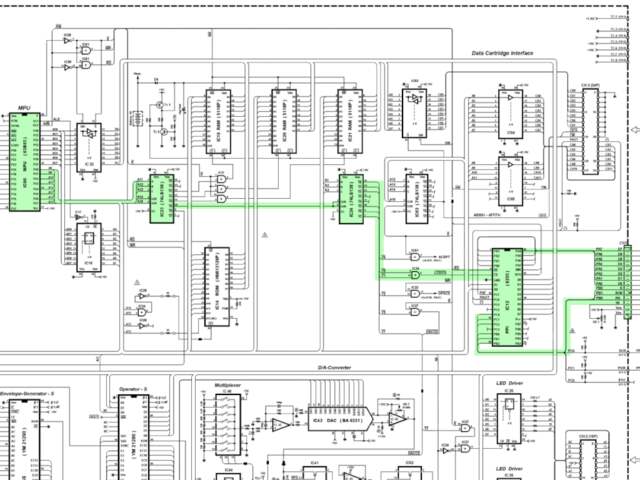
The best version of the schematics I’ve seen is
this
version, created by the yamahamusicians.com user Miks. While
you’re at it, grab a copy of the
service manual
too. We won’t be referencing it in this article, but it’s a good
resource to have. It explains certain details about the synth’s
architecture that aren’t obvious from the schematics.
Service Manuals:
Most consumer devices from the 80s and 90s have
service manuals available. These are technical documents
written by the manufacturer to assist in servicing the device. They
typically include schematics, diagrams, and lists of electrical
components. The first place to start when reverse-engineering a device
is looking for its service manual.
If you’re new to electronics, device schematics can look very
intimidating, but once you understand the basics they’re not actually
as scary as they look! You can find a good introductory guide to
schematics
here.
Background
But first, what does address decoding actually mean?
Address decoding
refers to how a specific device is mapped to a specific
address. In this section we’ll figure out what peripheral is mapped to
what address by tracing the address decoding logic in the synth’s
schematics.
The total amount of memory addresses that a CPU can access is referred
to as the CPU’s ‘address space’. This is limited by the
width of its ‘address bus’. The CPU’s address bus is
responsible for selecting addresses in attached memory devices, such
as RAM, or peripheral devices with addressable registers. Each
line in the address bus represents a single bit, with the total
number of lines determining the address range the CPU can access. For
example, a 16-bit address bus can address 216 unique memory
locations, or 64KiB.
When a CPU’s address lines are exposed externally in the form of pins
on the chip’s package, this is called an external address
bus. These lines can be physically connected to external memory devices.
Together with the CPU’s data bus, this allow reading and
writing binary data back and forth.
When the CPU performs an instruction that reads or writes memory, like
LDB 0x2001, several things happen:
-
The CPU’s external address pins are set to high and low
logic levels
according to the specified address. For address
0x2001
(0b0010_0000_0000_0001), address pins 0 and 13 will be
high, and all the others will be low. -
The CPU’s
RWpin will be set high to
indicate that this is a read operation, and… -
The CPU will prepare to accept the incoming data at
0x2001 over the data bus into the
B register.
But wait… If the CPU only has one set of address and data bus lines,
how do you connect multiple memory devices to the CPU? This is where
the
‘Chip Select’
interface comes in: Each device attached to the CPU’s data/address
buses has a ‘Chip Select’ pin, controlling whether the device responds
to incoming signals.
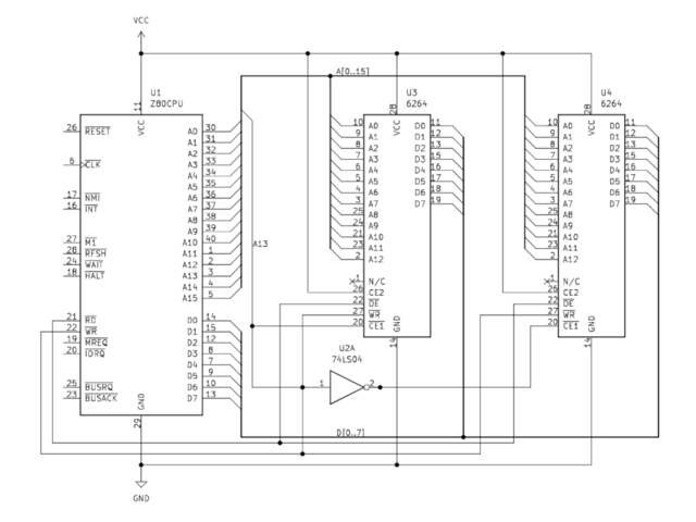
Consider the above (incredibly simplified) diagram: Two 8KiB
6264
RAM chips (U3 and U4) are connected to shared address and data buses
on a Z80 CPU. U3’s CE1 (Chip Enable)
pin is connected to the CPU’s A13 pin. The bar over the top of the
label indicates that this pin is ‘Active Low’, meaning a low
logic level will ‘activate’ its function. When the CPU selects an
address between 0x0 and
0x1FFF, the A13 pin will be low,
activating the U3 chip. U4’s CE1 pin
is attached to the CPU’s A13 pin via a NOT gate, which
inverts the signal coming from A13. When an address above
0x1FFF is selected, A13 will be set
high, selecting the U4 chip. This effectively maps U3 to the first
8KiB of the system’s memory, and U4 to the next.
Can you spot the problem with this example? Since any address
using A13 will ‘select’ U4, U4 is now mapped to every 8KiB
block of memory above 0x1FFF. In
reality, more sophisticated logic is used to map memory devices. Let’s
examine the real world example of the DX7’s address decoding
circuitry.
The DX7’s address decoding logic is primarily implemented via
the use of logic gates. If you’re not familiar with logic
gates, a good introduction to the topic can be found
here. Don’t worry though, we’re not going to be going too in-depth. A
basic understanding of what
AND, OR, andNOT gates do is all you need. One particular type ofcomponent you’ll encounter a lot inside vintage synthesisers are
7400-series logic chips.
Decoding the DX7’s Memory Map
#
Nearly all of the discrete electrical components that make up a DX7
are commonly available products. They’re mass-manufactured and sold by
a variety of different manufacturers. The best way to understand these
components is to read the datasheets made available by the
manufacturer. I’ll provide links to these as we go.
The creator of the DX7 schematics used the logic symbols ·
and + to denote
AND and OR gates, ratherthan the more standard
ANSI, or IEC notations [pdf]. Other gates use the ANSI notation.
The Firmware ROM
#
Let’s start by taking a look at the firmware ROM, IC14.
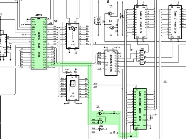
mapping logic highlighted.
In the schematic we can see that IC14’s
CE1 pin is connected to the CPU’s
A14/A15 lines via an AND gate, and a
NOT gate. What’s going on here?
The AND gate ensures that the signal is only high when
both address lines are active, and the NOT gate
inverts the signal so that it activates the active-low
CE1 pin. If A14 and
A15 being active on the CPU ‘selects’ the ROM chip, that
means it’s mapped to the address range
0xC000 – 0xFFFF.
Awesome! That wasn’t so hard. Now we know where the ROM is mapped in
memory. What’s next?
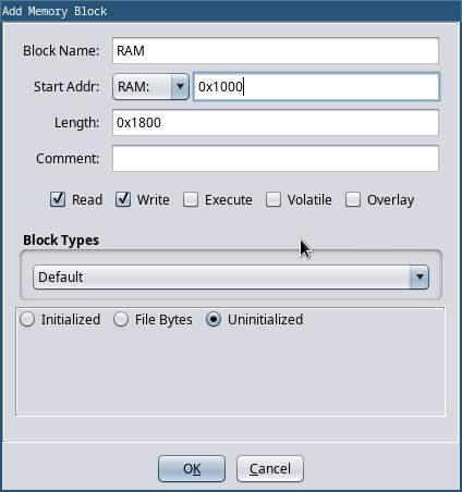
RAM #
The address decoding logic for the RAM is a little more complicated.
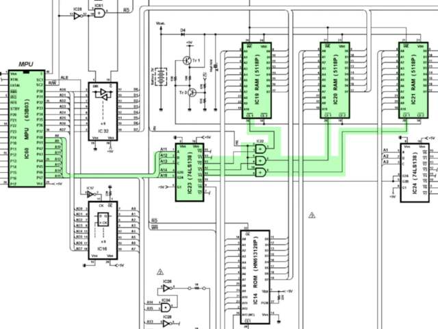
mapping logic highlighted.
The DX7 features three 4KiB
5118P
RAM chips (IC19, 20, 21). These are connected to the CPU’s address bus
via a
74LS138 demultiplexer
(IC23). This
demultiplexing
circuit is used to select one of 8 individual output lines based on a
3-bit input signal. These output lines are labeled as
Y0 –
Y7, and the input lines as DA, DB, and DC. The OR gates used here are wired to the system clock
output pin. Presumably to ensure the timing of read and write
operations are valid.
combinations of input lines select which output line.
The first RAM chip (IC19)’s chip select terminal is connected to the
demultiplexer’s
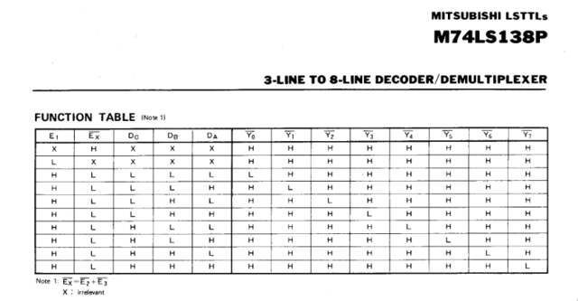
Y2 line. The ‘Function
Table’ from the 74LS138P datasheet shows that
Y2 will be set low when
input DB (connected to the CPU’s
A12) is high. Therefore, when the CPU selects address
0x1000, the first RAM chip will be
selected.
Y3
(connected to the second RAM chip, IC20) will be set low when inputs
DA and DB (A11
and A12) are high, corresponding to an address of
0x1800. Likewise,
Y4
(connected to IC21) corresponds to an address of
0x2000.
By tracing this address decoding logic, we’ve successfully mapped the
synth’s RAM to
0x1000 – 0x2800.
LCD Screen #
The last peripheral we’re going to look at right now is the synth’s
LCD screen. When you take your first peek inside a binary you’ll be
staring at an intimidating jumble of machine code. One of the few
things that will stand out at a glance is ASCII strings. A good way to
get a quick overview of the binary is finding out how these strings
are printed to the screen, and where.
The best place to start doing that is understanding how the CPU
interfaces with the LCD controller, and working your way backwards to
the code responsible for sending string data to it. Once you’ve found
how strings are printed to the screen, you can easily see
what’s printed where to get a better understanding
of the code.
mapping logic highlighted.
The LCD address mapping logic might look really complicated, but don’t
worry though. It’s just more of the same logic as before.
IC23’s Y5 pin is connected
to IC24, another 74LS138 demultiplexer. From the 74LS138 function
table we know that Y5 goes
low when inputs A, and C (A11 and A13) are
high. So it looks like IC24 is mapped to
0x2800.
Take a look at IC24: Inputs A, B and C are wired to
A1, A2 and A3. That means that
IC24 only maps 8 bytes.
IC24’s Y0 and
Y1 pins are connected to an
AND gate connected to the ‘chip select’ pin of IC12.
What’s happening here? This might seem a little confusing at first,
but since the 74LS138P’s outputs are active-low, this makes
LCDCS active when either
Y0 or
Y1 are active. This maps
IC12 to the four-byte range
0x2800 – 0x2803. Awesome. But what’s
IC12 doing?
IC12 is an
Intel 8255
Programmable Peripheral Interface (PPI). It provides 24
parallel, bidirectional IO lines.
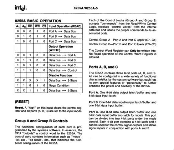
operations.
The schematics show the LCD’s parallel interface (DB0 - DB7) is connected to the PPI’s port A (PA0 - PA7), and its
control pins (E, RW and RS) to the PPI’s
port B (PB0 - PB2).
The Hitachi LM016 LCD screen used in the DX7 features the ubiquitous
Hitachi HD44780 LCD Controller. According to its datasheet (available
here) it has two registers. When its RS line (connected to
the PPI’s PB0) is low, the instruction register is
selected. When high, the data register is selected.
Based on the HD44780 datasheet, and the above table from the 8255’s
datasheet, we can tell that the LCD’s data register must be mapped to
0x2800, and its control register to
0x2801. We’ll go into more detail
about the LCD controller itself later in the article.
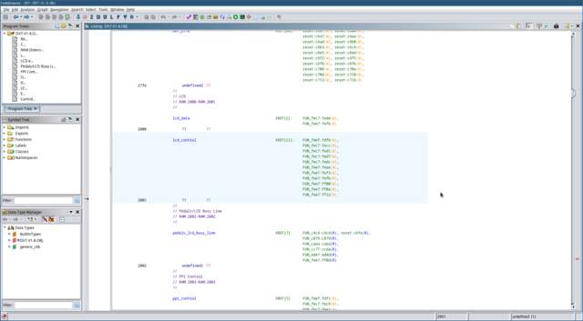
Wrapping Up #
Now we’ve got a pretty good idea of what’s going on where in the
memory map, and how this is discovered. To save you the trouble of
going through the whole schematic, here are all the memory-mapped
peripheral addresses.
| Address Range | Peripheral |
|---|---|
| 0x1000 – 0x2800 | RAM (External) |
| 0x2800 | LCD Data |
| 0x2801 | LCD Control |
| 0x2802 | Sustain/Portamento Pedals, and LCD Busy Line |
| 0x2803 | 8255 Peripheral Controller Control Register |
| 0x2804 | OPS Mode register |
| 0x2805 | OPS Algorithm/Feedback register |
| 0x280A | DAC Volume |
| 0x280E | LED1 |
| 0x280F | LED2 |
| 0x3000 – 0x4000 | EGS |
| 0x4000 – 0x5000 | Cartridge Interface |
| 0xC000 – 0xFFFF | ROM |
These aren’t the only peripherals attached to the system, the Hitachi
6303 CPU also features ‘IO Ports’. These are memory-mapped
input/output lines with their own dedicated functionality. We’ll touch
on these later in the article.
Disassembling The Firmware
#
Now that we know the memory map, we can start disassembling the
firmware. To do this we’ll use a graphical disassembler called
Ghidra. It’s a relatively new player on the scene, but it’s free, open
source, and very powerful. A great resource to keep handy while
working with Ghidra is the
Ghidra Cheat Sheet.
As of the time of writing, Ghidra doesn’t yet support the HD6303
architecture out of the box, so we’ll need to install our own language
specification.
This
repository contains a Ghidra language specification for the 6303
architecture. To install it, download the repository and copy the
6303 directory to theGhidra/Processors directory inside your Ghidrainstallation. You’ll need to restart Ghidra to see the new processor
in the list.
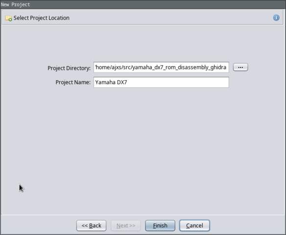
Once you’ve installed the language definitions, open Ghidra and create
a new project.
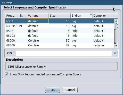
The first thing we’re going to need to do is to import the firmware
ROM binary. Select the ‘6303’ language, and click ‘OK’.
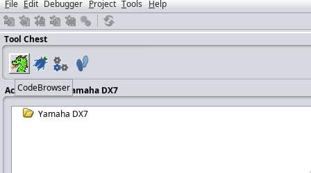
Next, open up the Codebrowser. This is where all the action
happens.
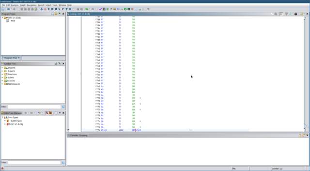
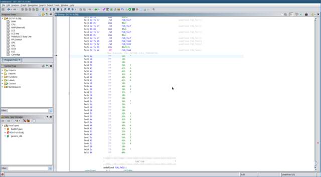
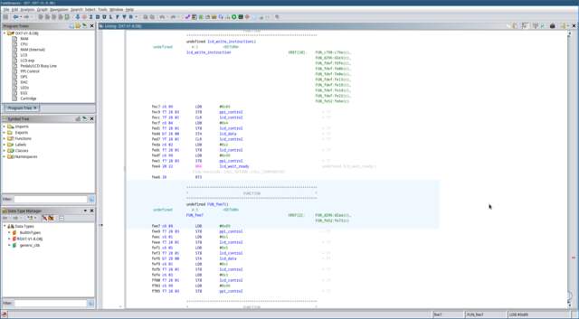
Once the initial disassembly loads, the first thing you’ll be looking
at is row after row of hexadecimal. This is the actual machine code as
it would appear to the CPU. Don’t bother with analyzing the
file.
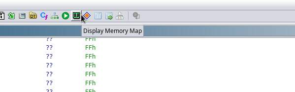
The first thing we’re going to do is set up the memory map. Remember
that thing we just did all that hard work figuring out? That’s going
to come in handy now. Press the ‘Display Memory Map’ icon in
the top button bar, to open up the Memory Map dialog.
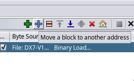
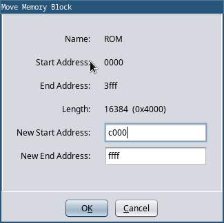
By default there’s only one memory block defined. This block consists
of the binary we just imported, so go ahead and rename it to
‘ROM’. The next thing we need to do is move this block to the
correct offset 0xC000. Because all of
the machine code instructions reference memory with absolute
addresses, if we didn’t map the ROM to the correct location none of
the disassembly would work.
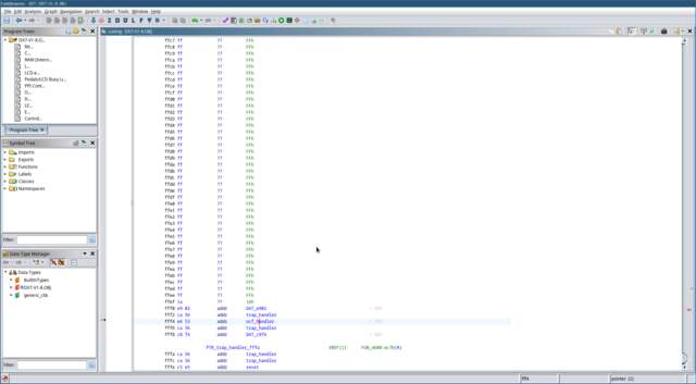
Before we finish setting up the memory map, let’s take a quick look at
the code. When the Hitachi 6303 processor in the DX7 powers up, it
knows where to begin executing code by fetching a pointer from a
specific location in the interrupt vector table.
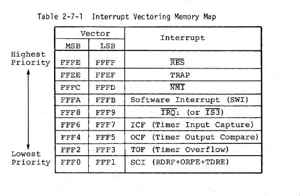
interrupt vector table.
In this case the ‘Reset vector’ is always located at the
specific memory address 0xFFFE, right
at the end of the address space. Press the
Ctrl+End
combination on your keyboard to move to the end of the binary, and
select the offset 0xFFFE by clicking
on it. Press the
P
key on your keyboard to convert the data at this address to a pointer.
You should see something similar to the image below.
Double-click on this pointer to take you to the associated offset in
the binary. Now we’ve found where the actual code is located, but it
doesn’t look like much just yet.
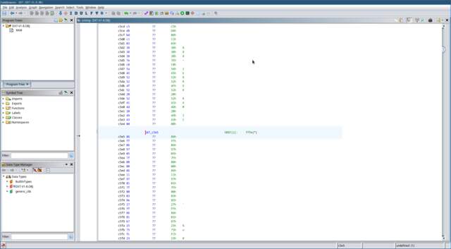
To begin disassembling the machine code into something we can work
with, click on the label and press the
D
key on your keyboard, or right-click and select
‘Disassemble’ in the context menu.
Different processor architectures will have different methods for
locating the reset handler. Typically a pointer to the reset handler
will be stored in an interrupt vector table (IVT) at a fixed
location in memory. On an ARM Cortex-M processor the IVT is located at
address 0x0, and the reset vector at
0x4. On the
MCS-51
architecture —another popular 8-bit microcontroller commonly
seen in synthesisers— the actual reset handler begins
at 0x0.
The disassembly process will follow the flow of code through the
binary, disassembling as it goes. An error will pop up here, but don’t
worry about it for now. This is just the disassembler mistaking a jump
table for code.
Once the disassembly completes you should see something like the
picture below.
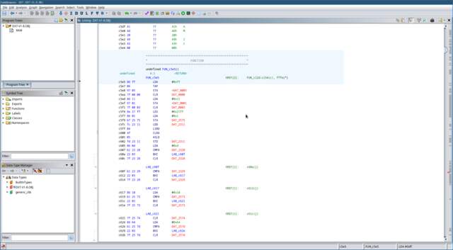
Now we’re looking at real code! No need to panic though. If you don’t
understand what you’re looking at, that’s okay. Assembly can look
pretty intimidating at first, but with a little bit of practice you’ll
get the hang of it!
Each of the lines you’re seeing here represents a single machine-code
instruction translated into assembly code. The three letter
mnemonics are the human-readable representation of the
instructions.
LDA
for example, is the mnemonic for the
‘Load value into register A’ instruction.
STA
is the mnemonic for the
‘Store value in register A’ instruction. If you’ve never
encountered assembly language before, that’s okay!
This
video will give a very quick and general introduction to assembly
language.
The HD63B03RP CPU used in the DX7 is a member of the
6800
family of processors. Its instruction set (the full set of assembly
instructions) is small and easy to understand. A great resource
for understanding the 6303 CPU and its instruction set is the
HD6301/HD6303 Series Handbook
freely available on bitsavers.org.
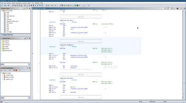
The FUN_c5e5 text you’re seeing
here is a label. This is a symbol placed in the disassembler’s
symbol table, which can be referenced elsewhere in the assembly code, usually as
the target for a branching instruction. Ghidra should already have set
up the reset vector as a ‘function’. Select this label with your
cursor and press the
F
key on your keyboard to edit the function and give it a more
meaningful label like
reset.
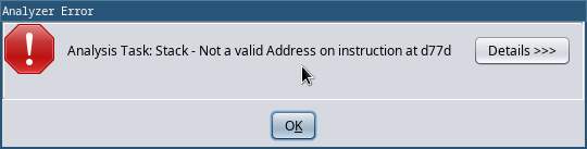
But what are all these red labels we’re seeing, like
DAT_2575?
If you try to double click on it, Ghidra offers a helpful error
message: ‘Address not found in program memory: 2575’. This is
because we’re missing our memory map! Let’s go back to the ‘Memory
Map’ dialog, and add the missing blocks.
Fill in the memory map that we worked out in the last section. The
completed map should look something like the screenshot below. You can
choose to consolidate some of these blocks if you like. It’s not super
important how the blocks are divided. What matters is that the blocks
cover all of the needed peripheral addresses.
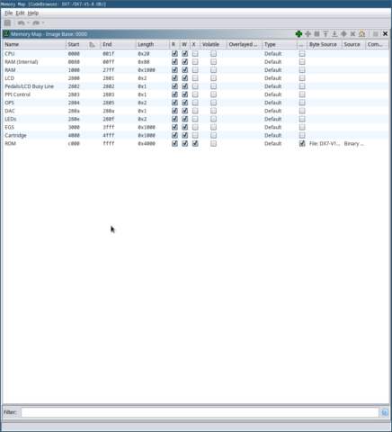
Note that I added memory blocks for the HD6303 CPU’s internal
registers, and internal RAM.
Now is a good time to go and fill in the individual peripheral
addresses that we know. The
HD6301/HD6303 Series Handbook
provides a list of the HD6303RP’s internal registers.
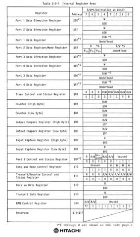
the IO port addresses.
Press the
Ctrl+Home
keys on your keyboard to go to address
0x0. Press the
B key
on your keyboard to declare that address
0x0 specifies a byte of data. You’ll
see the ?? change to db, which is the
assembler directive to define a byte of memory. Press the
L
key on your keyboard to give this address a useful label like
io_port_1_dir. Go ahead and fill
in the rest of the peripherals. When you go back to the reset handler
you’ll notice that, even with only a few pieces of the jigsaw puzzle
in place, things will start to make a lot more sense.
The Reset Function #
The main reset handler in the DX7 is responsible for initialising the
firmware. It sets up the CPU’s IO ports, ensures the firmware’s
important variables have valid values, and sets up the CPU’s
timer interrupt. More on this later.
The 6303 has three general-purpose
accumulator
registers: A,
B, and
D.
A and
B are both 8-bits in size, and
D provides a 16-bit view of both of
them combined:
D == (A << 8) | B.
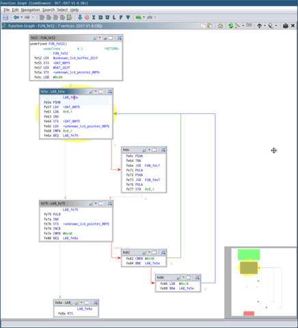
A great way to visualise the ‘control flow’ of the program is
in the ‘Function Graph’ view. This view shows a directed graph
of the program’s branching logic. You can open this view by selecting
Window → Function Graph in the top window menu. You
should see a view similar to the picture below.
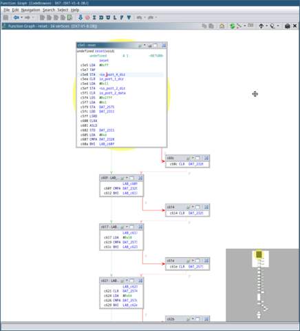
At offset 0xC605 you’ll see the
following instructions:
LDA   #0xd
CMPA  DAT_2328
BHI   LAB_c60f
-
The LDA instruction loads
the immediate value0xDinto the
A register. -
The CMPA instruction then
compares the value in the A
register with the value at the memory address
DAT_2328. -
The BHI instruction tells
the CPU to branch to the label
LAB_c60f
if the value in the A
register is greater than the value at
DAT_2328.
Condition Codes:
What actually happens when you execute a
CMPA
instruction is that the CPU sets a series of fields in the
‘condition code’ register based on the result of the
comparison. These ‘condition codes’ are used by the conditional
branching instructions to determine whether or not to take the branch.
In this case, the
BHI instruction will take
the branch if the C(arry) and Z(ero)
condition codes are both clear.
You can see in the function graph that if the memory at
DAT_2328
is greater than or equal to ’13’, it will not branch, and the value
will be cleared. The program will then continue to execute the next
instruction, which would have been the original branch target. In this
case, the program is checking to see that the ‘pitch bend range’
variable (stored in memory at location
0x2328) is within a valid range of
0-12. If not, it’s reset to 0.
If you look down at the bottom of the graph, you’ll notice something
interesting: The program goes into an infinite loop. This is the
firmware’s ‘main loop’.
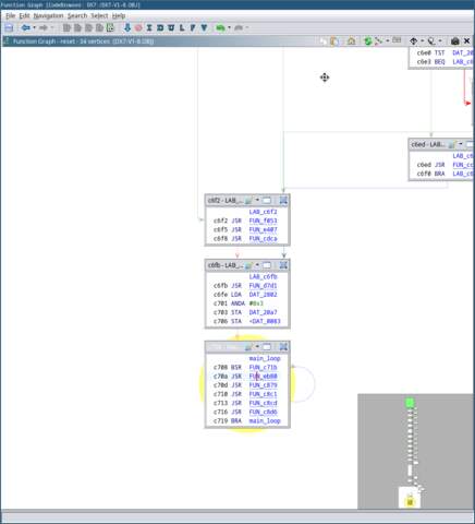
Tasks that need to be performed continuously happen here. Such as
updating the UI based on user input, and parsing incoming MIDI
messages.
When certain tasks not only need to be performed continuously,
but also periodically, there’s another way to make this happen:
interrupts.
Interrupts #
Interrupts
are signals sent to the processor by hardware or software to
interrupt the current code being executed, and handle a
specific event. They’re commonly used in embedded-software to handle
external, time-critical, or asynchronous events.
One of the most common types of interrupt you’ll encounter is a
‘timer interrupt’. The HD6303’s built-in timer interrupt consists of a 16-bit
‘counter’ register, which is incremented every clock cycle, and
a 16-bit ‘output compare’ register. When the value in the
counter register matches the value in the output compare register, a
timer interrupt will be raised. This causes the processor to halt what
it was doing, push the current state of the CPU onto the stack, and
jump to the appropriate interrupt handler specified in the interrupt
vector table. In the 6303 a pointer to this handler is located at
offset 0xFFF4. Once the firmware is
done handling the interrupt, it executes the
RTI instruction, which
restores the CPU’s state from the stack and continues executing the
code from where it left off.
The timer interrupt handler is where all the synth’s
real-time functionality happens. This is any code that needs to
be executed in a time-critical manner. The DX7 uses the periodic timer
interrupt to process portamento and modulation, update the individual
voice frequencies, and send the updated voice data to the sound chips.
Feel free to declare the pointer to the timer interrupt handler just
like we did for the reset handler, disassemble the handler, and take a
look at what’s going on.
LCD Interface #
One of the best places to start reverse-engineering a synth’s firmware
is to understand how it prints things to the LCD screen. We already
know where the LCD controller is mapped in memory, let’s work
backwards from there and see if we can find that code.
Press the
G key
on your keyboard to open the ‘Go To…’ dialog, and go to
address 0x2800.
These are the two memory-mapped LCD registers. The list of
cross-references on the right shows us where these addresses
are referenced in the code. Click on the
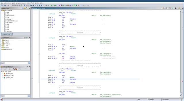
FUN_fdef label to take us to this
function. This is the function called by the reset handler to
initialise the LCD screen.
Below the function we can see something that looks like ASCII data.
In fact, it looks a lot like the welcome message displayed when you
boot up the DX7. Hmm. Click on offset
0xFE31, and press the
‘ key
on the keyboard twice. Once to convert the data at this offset to
character data, twice to convert it to a NULL-terminated string.
Notice that the welcome message location is referenced in the code at
offset
0xFE2B:
JSR   FUN_fe52
LDX   #0xfe31
JMP   FUN_fea4
Select the operand #0xFe31, and press
Alt+Ctrl+R
on your keyboard to turn this into a
memory reference. The default label looks a bit strange, so you
might want to give it a better one like
str_welcome_message
by selecting the reference and pressing the
L key.
We can see here that a pointer to the welcome message string is loaded
into the X register, and then the
ROM jumps to the function
FUN_fea4. Could this function have
something to do with printing the string? Let’s find out.
The Motorola 6800 family of processors has an interesting feature
called an
‘index register’. The index register (X) can be
used as a 16-bit base address, to which an 8-bit relative offset can
be applied. For example, the
LDA 4,x instruction willload the byte into A that is 4
bytes from the address stored in X.
This is useful because it allows us to reference 16-bit addresses with
only an 8-bit operand.
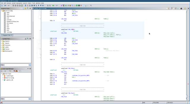
Let’s take a walk through FUN_fea4
together and see if we can figure out what it’s doing:
-
First, it pushes the address of the welcome message string in
X to the stack. -
Then it loads a memory address (0x261F) into X, and saves that address
to a pointer in memory. -
Then it restores the welcome message address from the stack into
X.
Not very helpful yet, unfortunately. Something I find that helps make
sense of so many unknown labels is to give them names that describe
how they’re used. Double-click on the label
DAT_00fb to go to its location.
Since we know this variable stores memory addresses, press the
P key
to convert it to a pointer. Giving it a name like
unknown_lcd_pointer_00fb
can help identify it at a glance later.
Use the
Alt+←
keyboard combination to navigate back to where we were before. Once
you’re there, click through to
FUN_fe8b.
We can see that lots of cross-references to this function have been
found in the code already. Let’s go through this function step by step
and see what we can figure out:
-
We already know that the
X register contains a pointer to
a string. So we can see that this function is loading an ASCII
character into register B from
the address stored in X. -
When the LDB instruction
loads a new value into B it sets
the condition codes according to its value. If the
most-significant bit of this byte is 1, the
N(egative) condition code will be set. This will cause the
BMI (Branch If MInus) instruction to branch. Valid
ASCII
values fall within the range 0-127, so this code looks like it’s
checking for an invalid character, and will branch to the exit if
this is the case.
Note: Different instructions treat integer values as either
signed, or unsigned, with the most-significant bit treated as the
sign bit. -
The value in B is then compared
against0x20(ASCII space). As I mentioned earlier, the
CMP instruction sets
condition codes according to the value in the associated
accumulator, and the operand. The
BCC instruction (Branch If Carry Clear) will branch if the C(arry) condition code is
clear. This means that the value in
B must be0x20or
above, otherwise the function exits.
You can read more about how the carry flag is used in computer
arithmetic on
Wikipedia. -
If the ASCII char is valid, it calls
BSR to branch to the
subroutine FUN_fe9a. In this
subroutine we can immediately see something interesting: Remember
that pointer we labeled earlier? This subroutine writes the ASCII
character in B
to the location in this pointer, increments the pointer, and saves
it… -
After this, the address in X is
incremented, and the function loops back to the start. Now the
function repeats, with X pointing
to the next character in the string.
Are you thinking what I’m thinking? This is a
String Copy function! It copies characters from a string into
a buffer, until either a NULL-terminator, or other unprintable ASCII
character is encountered.
Go ahead and give this function a label like
lcd_strcpy. If you like, you can
apply local labels to LAB_fe94,
and LAB_fe99 like
.copy_character and
.exit. Maybe give that buffer
address we saw earlier (0x261F) a
temporary label too.
You might have noticed the instructions
BSR
(‘Branch to SubRoutine’), or
JSR (‘Jump to SubRoutine’). These instructions are used to call subroutines. When a
subroutine is called, the address of the next instruction is
pushed onto the stack, and the
‘program counter’
jumps to the address of the subroutine. When the subroutine calls the
RTS instruction to
return to its caller, this address is popped from the stack
into the PC (Program Counter)
register, and the program continues from where it left off. Just like
a function call in a higher-level language.
This is where we’re at so far:
Let’s move on to that last function
FUN_fe52 and see where that leads
us. This function is a bit more complicated. Using the
Function Graph window I showed you before might help visualise
what’s going on.
Let’s go through this function step-by-step like we did before:
-
A new location in memory (0x263F)
is being saved to that pointer we saw before, and the LCD buffer
address we saw earlier (0x261F) is
being saved to a new pointer. There’s something interesting about
those addresses. They’re 32 bytes apart. That seems a bit
conspicuous, doesn’t it? Maybe this corresponds to the length of the
LCD screen (2 lines of 16 characters)? -
A constant value is loaded into
B. -
Inside the loop, we can see that
B is saved to the stack. A byte
is then loaded into A from the
location in the pointer at 0xF9. We
know from seeing the welcome message string loaded into
X
that this byte is ASCII string data. The pointer is then incremented
and saved. -
This byte is then compared against the byte pointed to by
unknown_lcd_pointer_00fb. -
If the character in
unknown_lcd_pointer_00f9 and
unknown_lcd_pointer_00fb
aren’t equal, then this character is used as an argument
for a function call to FUN_fec7.
The function at FUN_fec7 is a bit
more complicated, so I’ll walk you through what’s happening.
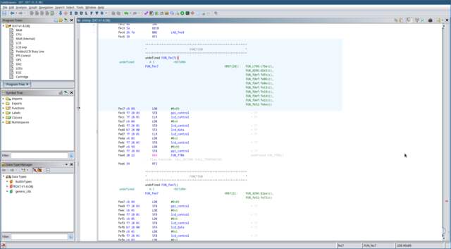
-
The constant
0x89is written to the 8255 PPI control
register at 0x2803. The PPI
datasheet refers to this as ‘Control Word #5’. This sets the
PPI’s Port A, and B to outputs, allowing the CPU to send data to the
LCD controller. -
A value of zero is written to the LCD control register. This sets
theRSline low to select the
Instruction Register, and theRWline low to
select a Write operation. -
The
Eline of the LCD is then driven high to instruct
it to be ready to receive data over the data bus. -
The byte in A is then written to
the LCD instruction register. After this, theEline is
driven low, and theRWline is driven high to signal
the end of the data transfer. -
The 8255 ‘Control Word #13’ is written to the PPI control
register to revert port A and C to being inputs. -
Finally, it branches unconditionally to
FUN_ff08.
Note about unconditional branches:
Sometimes, rather than returning with an
RTS instruction, a
subroutine will just unconditionally branch to the next subroutine. As
long as the stack is managed correctly, this is perfectly valid. The
second subroutine’s ending
RTS
instruction will just pop the original return value from the stack and
return to the original caller. This technique saves a few bytes of
code.
Let’s check out the subroutine at
FUN_ff08 that our function jumps
to.
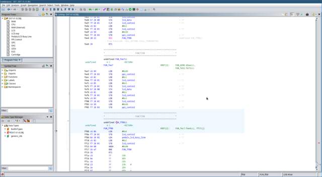
-
The
EandRWlines of the LCD controller
are set high. This sets the LCD controller to read mode. -
The PPI’s port C is read into the
A register, then the
Eline of the LCD controller is set low to indicate the
read operation is complete. -
A bitwise
ANDis performed between value of the
A register and
0b1000_0000. This checks the status of the
PC7line. If thePC7line is high, the
function loops back to the start.
It’s easy to miss, but if you look closely in the schematics you’ll
see that the PPI’s PC7 line is connected to
PA7, which is connected to the LCD controller’s DB7 pin.
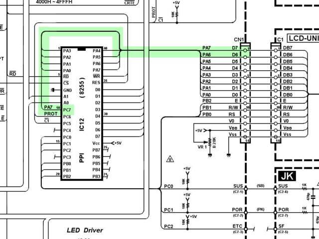
The DB7 pin serves as the LCD controller’s ‘Busy Flag’. This
flag indicates whether the LCD controller is busy processing data.
When it’s clear, the LCD controller is ready to accept new data.
It looks like the purpose of this function is to poll the LCD
controller, waiting for it to be ready to accept new data. Awesome!
Let’s give it a label like
lcd_wait_ready. Okay! So putting
it all together, the function at
0xFEC7 writes an
instruction to the LCD controller, and then waits for it to
be ready to receive data again. Go ahead and give it a name like
lcd_write_instruction.
Reverse-engineering often involves going down a rabbit hole. Sometimes
you need to fill in a few different pieces of the puzzle before you
can start to see the whole picture. Let’s return to the function at
FUN_fe52 and see what happens
next.
We now know the loop is writing an instruction to the LCD controller,
but what did this instruction do? The original instruction value when
the function started was 0x80, and it’s incremented by
one with each iteration of the loop. The HD44780 datasheet tells us
that 0x80 is the instruction to set the DDRAM (Display
Data RAM) address in the LCD controller. This is the address in the
LCD’s memory where the next character will be written. A value of
0x80 indicates the start of the screen’s first line.
The next function call (FUN_fee7)
looks almost identical to our
lcd_write_instruction function.
The only difference is that it writes to the LCD controller’s
data register, rather than the instruction register. This
must be where the actual character data is written! You can give this
function a label like
lcd_write_data. Note that this
function ‘falls-through’ to the LCD controller polling function
we saw earlier.
Now we know what’s going on here. This is our LCD printing function!
Notice that after writing the character data to the LCD, at offset
0xFE77 the function writes it to the
buffer at 0x263F? The incoming
characters are compared against the contents of this buffer to see if
they’re identical, if they are then it skips printing the character.
Maybe these buffers represent the ‘next’, and
‘current’ contents of the LCD screen?
After writing the LCD character data, the function then checks whether
the LCD instruction byte is equal to 0xD0. Now we know
that this is checking whether the LCD DDRAM position is at the end of
the second line. If not, it checks whether we’re at the end of the
first line (0x90). If so, the instruction byte is set to
0xC0, which sets the DDRAM address to the start of the
second line.
Note about HD44780 DDRAM addresses:
Each ‘line’ in the HD44780 LCD controller actually has a length of 64
characters, even if the screen is only 16 characters wide. As a
result, 0xC0 (0x80 + 0x40) is the correct
DDRAM address for the start of the second line.
Awesome! Now we’ve discovered the LCD printing function! Go ahead and
give it a name like lcd_print.
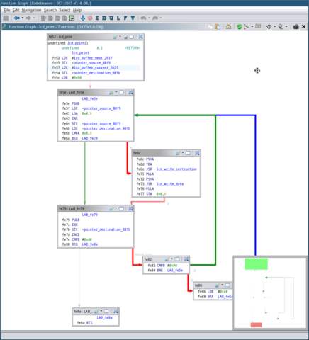
lcd_print function. Note that I went
ahead and labelled all of the important variables.
If you’ve followed along, give yourself a huge pat on the back. This
was no easy feat! You’ve now got a pretty good understanding of how
vintage synth binaries are reverse-engineered. Everything else
involved in disassembling a synth’s firmware is just a matter of
applying these same ideas.
The HD44780 LCD controller has been a staple in consumer devices for
decades. LCD controllers compatible with the HD44780 instruction set are
still being manufactured, and are commonly used in commercial, and
hobby projects alike. Because of this, lots of tutorial material is
available online, and the knowledge gained in working with it is
applicable elsewhere.
Going Further #
The MIDI Handling Routine
#
After disassembling the LCD printing function, the next best way to
figure out what’s going on inside a synth ROM is to disassemble the
function that parses incoming MIDI data. This function is an entry
point to nearly every aspect of a synth’s functionality. Disassembling
it will allow you to trace the path of a particular MIDI message to
its associated functionality. You can trace ‘NOTE ON’ and
‘NOTE OFF’ messages to find the code that handles starting and
stopping individual voices; Or you can trace
‘CONTROL CHANGE’ messages to find the code that handles pitch
bend or modulation.
I decided not to tackle this function in this article, as the DX7’s
MIDI parsing code is huge, and requires a lot of explanation. Parsing
MIDI messages is always implemented via a straightforward state
machine, and the code is nearly identical across different synths.
Once you’ve seen how it works in one synth, you’ve seen how it works
in nearly all of them.
Debugging the Firmware in an Emulator
#
One of the best ways to understand what’s going on inside a synth’s
firmware is to run it in an emulator. The
MAME
emulation framework is freely available, and already supports a wide
variety of vintage synths. It features a built-in disassembler, and a
debugger that can be used to step through the firmware instruction by
instruction to see what’s happening in detail. When I was working on
my
Yamaha DX9/7
project, I used MAME as a testing and development platform for the
firmware.
Final Words #
The DX7, and its 8-bit CPU might be a bit primitive by today’s
standards, but the same principles apply to reverse-engineering modern
devices. Instructions sets and
calling-conventions
might change, but whether it’s a vintage 8-bit architecture like the
6800, or a cutting-edge 32-bit ARM system, the principles of how to
disassemble device firmware remain the same.
If you have any questions about this article, please get in touch! If
you have any corrections or suggestions, I’d love to hear from you.
Thank you for reading!
Appendix: Why Choose This Synth?
#
It Can Be Disassembled With Free Software
6303 binaries can be disassembled by using free and open source tools,
such as Ghidra,
F9DASM, and MAME’s
Universal Disassembler.
It’s Well Documented
40 years on, the DX7 continues to captivate people’s imaginations. As
a result, lots is known about what goes on inside a DX7. Yamaha’s
service manuals are comprehensive, and freely available online.
Yamaha even released internal documentation on the DX7’s architecture
and sound chips, which is now
available online.
Only One ROM
One advantage of reverse-engineering the DX7 is that there’s only one
ROM you need worry about.
Technically there’s also the sub-CPU and its mask ROM, but in
this case you don’t really need to worry what’s going on
there.
Some synths have important part of the firmware stored on the CPU’s
mask ROM, such as the Casio CZ-101. Other synths spread the synth’s
core functionality across multiple CPUs, each with their own ROMs,
such as the Roland JX-8P. The DX7 is much simpler, having (nearly) all
of its code in one place.
It Has an LCD Screen
Disassembling code for a system with a text-based user interface has a
lot of advantages. I considered some of the early DCO-based Roland
polysynths as candidates for this article, but without an LCD screen
it’s much harder to make headway into a ROM.
No Bank Switching
Unfortunately the various disassembler tools available don’t handle
bank switching
very well. In Ghidra you can use ‘Overlay’ memory blocks to set up the
different banks, however it’s still not very intuitive in my
experience.
I considered the Ensoniq ESQ-1 as a candidate for this article. It
features a Motorola MC6809 processor, which is very well supported by
lots of different debuggers. However it uses bank switching, which
makes it a bit of a nuisance to disassemble.
What Is Bank Switching?
What happens if you need to squeeze 64KiB of firmware ROM, and 32KiB
of RAM into your HD6303 chip’s 16-bit address space? One solution to
this problem is bank switching. Many vintage synths use
bank-switching to fit their firmware into the CPU’s address space.
Bank switching breaks a memory device’s address space up into multiple
‘banks’
by latching one or more of its address lines to one of the CPU’s I/O
port lines. This allows the CPU to select which ‘bank’ is active by
toggling the aforementioned I/O line in the software.
and RAM wiring.
The Yamaha TX81Z features a 64KiB 27C512 EPROM chip, mapped into the
CPU’s address space at
0x8000 – 0xFFFF. The EPROM’s A0-A14
pins are wired to the CPU’s A0-A14, and the EPROM’s
CE1 pin is latched to the CPU’s A15
pin. The EPROM’s A15 pin is wired to the CPU’s I/O port 6 (pin
P63 in the schematics). If the P63 I/O line
is pulled high, the upper half of the EPROM’s memory is
selected, mapping addresses
0x8000 – 0xFFFF into the CPU’s
address space. If it’s pulled low, the EPROM’s
0x0000 to 0x7FFF memory is mapped to
0x8000 – 0xFFFF.
To allow branching from code in one bank to code in another, a common
technique is to use a
‘trampoline function’
located at the same address in both banks.
Appendix: Documentation
#
Below is a list of all the important documentation referenced in the
article.
⚡ Tell us your thoughts in comments!
#️⃣ #Introduction #ReverseEngineering #Vintage #Synth #Firmware
🕒 Posted on 1760938309